In situ deposition/positioning of magnetic nanoparticles with ferroelectric nanolithography
- PDF / 1,009,411 Bytes
- 7 Pages / 612 x 792 pts (letter) Page_size
- 67 Downloads / 256 Views
Ferroelectric nanolithography is a new approach to processing nanostructures, which can position multiple components made of various materials into predefined configurations. Local polarization in ferroelectric compounds is manipulated to control the surface electronic structure and direct attachment of molecules and particles. Here, the presence of optically excited electron-hole pairs on ferroelectric domains is confirmed, and reaction paths for photo reduction of several reactive metal particles are determined. Subsequent and simultaneous deposition of multiple metals is demonstrated, and the magnetic properties of Co based particles are confirmed.
I. INTRODUCTION
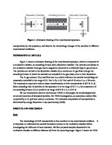
Over the last five years there has been an explosion in the synthesis of new functional nanostructures, i.e., tubes, wires, dots, synthetic biological molecules, etc.1 To exploit these structures in devices, concomitant advances in materials processing are required. Interesting approaches have been developed for some specific applications. The first nanolithographies were based on scanning probes, which are not considered practical, except in specific niche applications.2 Microcontact printing has become a common method of patterning self-assembled monolayers.3 Nanoimprint lithography and “step and flash” lithography have been developed to pattern semiconductor photo resists.4,5 DNA and protein directed assembly have been used to control nanoparticle assembly.6–8 Dip-pen lithography and similar approaches based on ink jet printer strategies are finding use in specific applications such as array chips.9,10 Finally electric, magnetic or mechanical fields have been used to align nanostructures, for example as is practiced in electrophoretic assembly.11,12 These strategies are successful in producing patterns or arrays of particles, molecules, wires, or tubes, generally operating on one class of material at a time. Recently Kalinin et al.13 proposed a directed assembly process, ferroelectric nanolithography, which can position multiple components made of various materials into predefined configurations. The approach is based on observations of orientation- and domain-dependent chemical reactivity.14–16 Ferroelectric nanolithography utilizes
a)
Address all correspondence to this author. e-mail: [email protected] DOI: 10.1557/JMR.2005.0093 712
J. Mater. Res., Vol. 20, No. 3, Mar 2005
atomic polarization in ferroelectric compounds to control the surface electronic structure and direct attachment of molecules and particles. The earlier work demonstrated the process on photo reduction of inert metals to produce nanometer-sized particles and attachment of functionalized organic molecules. The process has the potential to be completely general, operating on reactive metals, functionalized nanowires, tubes, and dots as well as biological molecules, but these processes have not yet been demonstrated and are not understood at a fundamental level. This paper reports the controlled patterning of cobalt-, nickel-, and iron-based nanoparticles, subsequent and
Data Loading...