In Situ Observations of Misfit Dislocations in Lattice-Mismatched Epitaxial Semiconductor Heterostructures
- PDF / 1,534,372 Bytes
- 6 Pages / 576 x 792 pts Page_size
- 45 Downloads / 340 Views
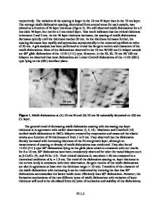
large fraction of the layer melting temperatures (e.g., Reference 3)); and (3) introduction of a dislocation network into the substrate/epilayer interface, which as shown schematically in Figure lb, will allow the epitaxial layer to relax toward its bulk lattice parameter. This dislocation mechanism is the most prevalent strain relaxation mechanism at typical crystal growth and processing temperatures, and we concentrate on this mechanism in our experimental studies. For a given materials system and lattice The Fundamental parameter difference, there will be a charScientific Issue acteristic thickness, known as the critical It is well established that it is possible thickness hc, at which the introduction of to grow a thin, coherent epitaxial layer on an interfacial misfit dislocation array bea substrate with a slightly different lattice comes energetically favorable. The critiparameter, as illustrated in Figure la. This concept is known as strained layer epitaxy. cal thickness was first4 predicted by Frank and van der Merwe, and a generally acIn the fields of semiconductor physics and cepted model by Matthews and Blakeslee5 device design, strained layer epitaxy ofpredicts: fers many exciting new opportunities (see Reference 1 for a review). A coherently hc = [ln(ahc/b)][b(l strained structure, however, will store an enormous elastic strain energy density in (1) /[87re(l + i^cosA the epitaxial layer, due to the distortion of interatomic bonds. Therefore, as the epiIn Equation 1, v is the epilayer Poisson taxial layer increases in thickness during ratio, b is the magnitude of the misfit disgrowth, it will become increasingly enerlocation Burgers vector, e is the strain arisgetically favorable to relax this strain ening from the lattice parameter difference ergy. A number of relaxation routes exist: between substrate and epilayer, A and (1) roughening of the epitaxial layer surface are angular factors, and a is a factor de(see, for example, Reference 2); (2) interdifscribing the dislocation core energy. The fusion of the layers (this will generally only predictions of this model for the Ge^Sii _x/ be significant at temperatures which are a Si(100) system are shown in Figure lc. This 32
particular heterostructure has been widely studied as a "model" system and we shall concentrate on it in this review. The lattice mismatch varies continuously with Ge concentration x in the GexSij - x alloy, with a strain e = 0.041x. Also shown are experimental measurements of hc for crystal growth temperatures of 550°C,6 750T,7 and 900°C.8 There is substantial deviation between theory and experiment at lower lattice mismatches and growth temperatures. These discrepancies are due primarily to kinetic factors inhibiting the formation of the misfit dislocation array.9~u In particular, the energetic barriers involved in the formation and motion of misfit dislocations are typically > > kT. Thus, at lower temperatures misfit dislocation nucleation and growth rates will be much lower, resulting in an "incubation time" as the misfit dislocat
Data Loading...