Misfit Dislocations at Mismatched Epitactic Heterojunctions
- PDF / 3,526,989 Bytes
- 6 Pages / 420.48 x 639 pts Page_size
- 96 Downloads / 378 Views
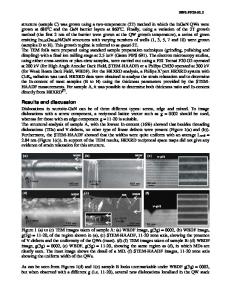
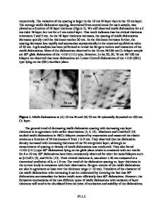
MISFIT DISLOCATIONS AT MISMATCHED EPITACTIC HETEROJUNCTIONS Jane G. Zhu, C. Barry Carter and Chris J. Palmstrom* Department of Materials Science and Engineering, Cornell University, Ithaca, NY 14853 *Bellcore, 331 Newman Springs Road, Red Bank, NJ 07701 ABSTRACT The formation and structures of misfit dislocations are significant factors in understanding heteroepitaxy of lattice-mismatched materials. In this study, GaAs/Si, CoGa/GaAs and ErAs/GaAs heterojunctions in materials grown by molecular-beam epitaxy have been characterized using transmission electron microscopy. Different types of misfit dislocations have been generated at these interfaces. The different dislocation configurations are discussed, along with interactions between 60" and 90" dislocations in GaAs/Si heterojunctions; the 600 dislocations might be associated with surface steps or edges of islands. The growth of antiphase boundary structures in the CoGa and ErAs grown on GaAs are proposed. INTRODUCTION The development of compound-semiconductor devices invariably involves lattice mismatched heteroepitaxy. Mismatched systems involving two semiconductors (zinc-blende or diamond structure), such as GaInAs/GaAs, CdTe/GaAs, GaAs/Si and GeSi/Si, have been extensively studied [1]. Recently, these studies have been extended to systems where one side of the heterostructure is a metal or semimetal, such as the transition-metal aluminides [2] and gallides [3,4] (CsCl structure) and the rare-earth monopnictides [5-9] (NaCl structure). At the mismatched heterojunctions, misfit dislocations are formed to accommodate the lattice mismatch when the epilayer thickness is beyond a particular "critical" value. These dislocations do not always remain at the interface. Instead, some of them thread through the epilayers and thus affects the electrical or optical performance of the epilayer. Many different models have been employed to predict the critical thickness [10-13]. However, the experimental data concerning critical thicknesses do not always agree with the prediction from the existing theories. Further studies where the mechanism of the nucleation of misfit dislocations is identified for different mismatched heteroepitactic systems are necessary. This paper summaries results of several recent studies on a variety of mismatched systems involving the diamond, zinc-blende, CsCl and NaCl structures and discusses dislocations and defects at the heterojunctions. Specific examples of GaAs/Si, CoGa/GaAs and ErAs/GaAs are illustrated. These epilayers were grown by molecularbeam epitaxy (MBE) on (100) substrates and characterized by transmission electron microscopy (TEM). MISFIT DISLOCATIONS In most studies of heterojunctions between III-V or group-IV semiconductors, the misfit dislocations form a network of two sets of orthogonal dislocations, as in the case of GaAs/Si [14], since the common growth plane is (100). The Burgers vectors of these misfit dislocations are a/2 since this is a lattice vector for both crystals at the heterojunction. However, the structure of misfit
Data Loading...