In Situ Surface Passivation of GaAs by Thermal Nitridation using Metalorganic Vapor Phase Epitaxy
- PDF / 377,231 Bytes
- 6 Pages / 420.48 x 639 pts Page_size
- 58 Downloads / 298 Views
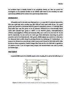
"**Departmentof Chemistry University of Wisconsin-Madison Madison, WI 53706 ABSTRACT An ammonia-based, in situ passivation of GaAs surfaces conducted within a metalorganic vapor phase epitaxy reactor is present. The shift of the GaAs surface Fermi level, and hence the surface charge density, resulting from this in situ passivation, has been studied using photoreflectance (PR) spectroscopy. Samples consisting of an undoped GaAs layer on highly doped n-GaAs (UN+) and p-GaAs (UP') structures allow for the exact determination of the surface Fermi level position using PR These structures were grown by MOVPE and in situ thermal nitridation was performed after growth within the MOVPE system without exposure to the air. After nitridation, the surface Fermi level can be shifted by - 0.23 eV towards the conduction band edge for UN' structures and by - 0.11 eV towards the valence band edge for UP' structures from the normally mid-gap 'pinned' positions. INTRODUCTION Compound semiconductors, such as GaAs and InP, are widely used for high-speed semiconductor devices as well as other microelectronic and optoelectronic devices. Most Il-V compound semiconductors, particularly GaAs, possess a high density of midgap surface states that have complicated the development of many potential applications- Surface passivation is therefore an important process in the fabrication of GaAs-based electronic devices. The nitridation of GaAs surfaces can result in the formation of a thin nitride-based surface layer. This thin nitride-based layer can act as an effective surface passivation layer which can reduce the surface state density and hence improve the device performance [1, 2]. The Fermi level position at GaAs surfaces is a crucial property, however, the shift of surface Fermi level due to thermal nitridation has not yet been systematically studied. In this study, we report on an in situ surface passivation of GaAs by thermal nitridation within a metalorganic vapor phase epitaxy (MOVPE) system. In situ nitridation of the GaAs surface after growth allows for a controlled chemical process on a surface free of oxide contamination. The in situ nitridation also provides the possibility of depositing subsequent layers, such as silicon nitride or silicon dioxide, immediately after nitridation of the GaAs surface. We have studied the shift of GaAs surface Fermi level, due to in situ thermal nitridation, using photoreflectance spectroscopy (PR). PHOTOREFLECTANCE SPECTROSCOPY PR has been shown to be a very useful method for determining the surface electric field and hence the surface Fermi level [3]. The special structures, proposed initially by Van Hoof et al. [4], are used to simplify the data analysis and ascertain the GaAs surface Fermi level position in 15 Mat. Res. Soc. Symp. Proc. Vol. 573 c1 999 Materials Research Society
GaAs
NPGaAs Light off
-
I
"Light
on Conduction Bandan
jNW mdopd Gas GUAM N+
ULi
Su0)traGa constant surface electric field in
L GaAs LL EF
. VB
.
.
•
.""' --.
this work. These structures consist of a thin la
Data Loading...