In-Situ Transmission Electron Microscopy Investigation of Aluminum Induced Crystallization of Amorphous Silicon
- PDF / 3,125,067 Bytes
- 7 Pages / 612 x 792 pts (letter) Page_size
- 19 Downloads / 384 Views
1066-A15-05
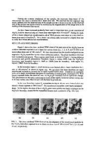
In-Situ Transmission Electron Microscopy Investigation of Aluminum Induced Crystallization of Amorphous Silicon Ram Kishore1, Renu Sharma2, Satoshi Hata3, Noriyuki Kuwano3, Yoshitsuga Tomokiyo3, Hameed Naseem4, and W D Brown5 1 Electron Microscope Section, National Physical Laboratory, Dr KS Krishnan Road, New Delhi, 110012, India 2 Center for Solid State Science, Arizona State University, Tempe, AZ, 85287 3 ASTEC, Kyushu University, Kasuga, 816-8580, Japan 4 Electrical Engineering Department, University of Arkansas, Fayetteville, AR, 72701 5 Electrical Engineering Deprtment, University of Arkansas, Fayetteville, AR, 72701 ABSTRACT The interaction of amorphous silicon (a-Si) and aluminum (Al) has been examined using in-situ transmission electron microscopy. Carbon coated nickel grids were used for depositing thin (~50nm) amorphous silicon films using ultra high vacuum cluster tool and a thin film of Aluminum (~50nm) was deposited subsequently on a-Si film by sputtering. The grid containing a-Si and Al films was mounted on a heating holder of FEI 200kV TEM and loaded in the TEM for viewing the microstructural and phase transformations during the in-situ heating process. The microstructural features and electron diffraction patterns in the plain view mode were observed with increase in temperature starting from 30 oC to 275 oC. The temperatures used in this experiment were 30, 100, 150, 200, 225, 275oC . A sequential change in microstructural features and electron diffraction pattern due to interfacial diffusion of boundary between Al and amorphous Si was investigated. Evolution of polycrystalline silicon with randomly oriented grains as a result of a-Si and Al interaction was revealed. After the in-situ heating experiment the specimen was taken out and etched to remove excess of Al and the subjected to high resolution imaging under TEM and EDS analysis. The EDS analysis of the crystallized specimen was performed to locate the Al distribution in the crystallized silicon. It has been shown that Al induced crystallization can be used to convert sputtered a-Si into polycrystalline silicon as well as nanocrystalline silicon at a temperature near 275 oC by controlling the in-situ annealing parameters. The mechanism of AIC has been discussed from the experimental results and the phase diagram of Al-Si system. INTRODUCTION Interaction of amorphous silicon with aluminum results in the formation of nano-, micro- and polycrystalline silicon at low temperatures. These materials are important due to their application in thin film transistors (TFTs), active matrix liquid crystal displays (AMLCD), solar cells and various other applications. Aluminum-induced crystallization (AIC) and doping of a-Si:H has been of great interest [1-6] because of its ability to produce polycrystalline silicon with good crystallographic and electrical properties at low temperatures. It is believed that dissolution of Al atoms in a-Si may weaken the Si bonds and enhance nucleation
and grain growth. We had shown in our earlier work [3,7] t
Data Loading...