Indentation-Induced Debonding of Ductile Films
- PDF / 3,890,285 Bytes
- 6 Pages / 417.6 x 639 pts Page_size
- 31 Downloads / 342 Views
Mat. Res. Soc. Symp. Proc. Vol. 586 © 2000 Materials Research Society
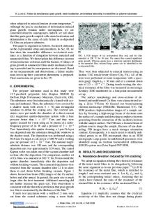
adhesion of Cu thin films with and without a 10 nm Ti adhesion-promoting underlayer as a
function of Cu film thickness (Figure 2). On average, for Cu (under 100 nm thick) without a Ti underlayer, 0.8 JIm 2 was measured. This value corresponds to the thermodynamic work of adhesion of Cu to SiO 2 (WT) measured by the contact angle technique [6]. This means that for films less than 100 nm thick there is almost no plastic deformation at the crack tip [3, 5]. For thicker films there is a definite contribution of crack tip plastic deformation (Uf) to the practical
work of adhesion (Wp), which scales with the film thickness (Figure 2). 1000
W, compression Cu, tension Ti
W Cu
INXINXIXXXN 4M,4%NON#& WN 4
SiO2 Si
Ai&
Figure 1. Thin film system.
0.8 J/m2 0"0•
as a function adhesionticknss.Cu Figure 2. Cu film of flm
.. I
0.1 Cu Fil T
, ..
1
Film Thickness, gxm
of film thickness.
10 10
For Cu on TiW, the thermodynamic work of adhesion is 2.2 JIm2 [6], which is about half the measured practical work of adhesion of Cu thin films with Ti underlayers. Following [3], the plastic zone size at the crack tip can be calculated if thin film adhesion is known: G =R,a' ýlysn (Rp )_11
(2),
where G is thin film's practical work of adhesion, E and ays are it's Young's modulus and yield stress, b is the Burger's vector, and Rp is the plastic zone size at the crack tip. Given the practical
work of adhesion of 4 J/m2 and 620 MPa Cu yield stress [9], the plastic zone size at the crack tip
is calculated to be 12 nm for Cu film under 100 nm thick with a Ti underlayer. Though the
TiW/Cu and the Ti/Cu interfaces are different, it seems that there may be a plastic term contribution even for the thinnest Cu films with a Ti underlayer. Based on the knowledge of film yield stress, several models were proposed to quantify Cu film adhesion as a function of film thickness [3, 5, 7].
FIDUCIAL MARKS In our previous study [4] circular crack arrest marks (fiducial marks) were found on the substrate side, and corresponded exactly to the blister original diameter. The marks' geometry was proposed to represent the crack tip opening angle (CTOA). Based on the CTOA measurements the tearing modulus can be calculated using Rice, Drugan and Sham (RDS) analysis [11]. From this the steady state strain energy release rate was calculated for thin Cu films in terms of the thermodynamic work of adhesion [4]. For Cu films under 100 nm thick the
256
true work of adhesion was only a 27% higher than the thermodynamic work of adhesion, which perfectly agreed with the actual experimental measurements (Figure 2). Conceptually it is important to know along what interface the fracture occurs during the blister formation. To evaluate this blisters were removed with carbon adhesive tape for analysis. Auger electron spectroscopy analysis showed that the failure occurs along the Cu/SiO 2 interface [4]. The delaminated area of a 120 nm thick Cu film after blister removal is shown in Figure
Data Loading...