Index of Refraction and Strain Induced Birefringence of Pseudomorphic Si 1-x Ge x
- PDF / 389,650 Bytes
- 6 Pages / 414.72 x 648 pts Page_size
- 108 Downloads / 299 Views
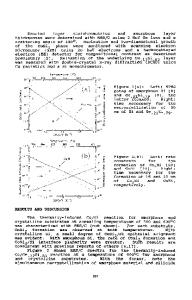
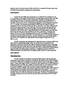
,5]. In this work we present measurements of the refractive index of pseudomorphic Sij.Gex for Ge concentrations between x = 0.01 and x = 0.09, at both ),=1330 nm and ,l=1550 nm. Our index measurements show that TE -TM birefringence of Si-. 1 Gex waveguides is dominated by the strain induced birefringence of the SitGeK epilayer. This strain effect is so large that it is a significant factor in Si1 .•Ge• waveguide performance. EXPERIMENT The Si/ Sii-,Gex /Si waveguides were grown on (001) Si substrates using ultra-high vacuum chemical vapour deposition (UHV-CVD) or molecular beam epitaxy (MBE). Each waveguide consists of the Si substrate, a Sii.xGe. guiding layer, and a Si cap layer. The layer thickness and Si1 .•Ge. concentrations for each waveguide are given in Table I. The thickness of the Si1 .•Gex layers was chosen to be smaller than the metasable limit (at the growth temperature), above which dislocations begin to form. The Sii.xGex layer thickness was measured by scanning electron microscopy (SEM), and X-ray diffraction was used to verify the Ge concentration of the waveguide layers and to confirm that the Si•.xGe, layers were fully strained. Absolute measurements of the refractive index are difficult to make because pseudomorphic Si 1.,Gex only exists in the form of extremely thin epilayers on Si substrates, and the index step, An, between the Sii.xGex and the underlying Si is very small. However, the mode profile in a Sil.xGex waveguide is uniquely determined by the magnitude of An. Hence An can be determined simply by fitting a calculated waveguide mode profile to the measured profile. In our experiments, the mode profiles of the Si.iGe• waveguides were measured using one of two techniques. In both configurations, an input optical fiber is used to couple either TE or TM polarized light into the waveguide. Two tunable external cavity semiconductor lasers were used as incident light sources, one tuned to X=1550 nm and the other to X=1330 nm. The first method uses a second tapered optical fiber to scan the output facet of the waveguide. This fiber is mounted on a computer controlled piezoelectric stage and positioned near the waveguide output facet. The rounded end of the fiber tip acts as a very short focal length lens. When the waveguide facet is positioned at the focal plane of the fiber tip, light is collected from a spot size of approximately 2 gm at the facet. The mode profile is collected by scanning the fiber tip vertically while monitoring the light intensity coupled into the fiber. Table I. The layer thickness and Ge concentrations of the SilxGe, waveguides used for refractive index determinations. Wafer A B C D E F
Sil.xGex layer Ge conc. thickness (pm) (mol. fraction, x) 0.97 +0.05 0.012 ±0.001 1.0 ±0.05 0.019 ±0.001 1.0 ± 0.05 0.026 ±0.001 0.50 ±0.02 0.036 ±0.001 0.28 ±0.01 0.070 ±0.001 0.193 ±0.005 0.090 ±0.001
102
Si cap thickness (pm) 1.01 ±0.05 1.0 ±0.1 0.85 ±0.05 1.7 ±0.1 1.5 ±0.1 1.5 ±0.1
Growth technique MBE UHV-CVD MBE MBE UHV-CVD MBE
Si -xGex
Iosr..I IiZ I, 1i sbstrate *
Air
exper
Data Loading...