Roughness Analysis of Si 1-x Ge x Films
- PDF / 2,831,240 Bytes
- 10 Pages / 414.72 x 648 pts Page_size
- 96 Downloads / 356 Views
ABSTRACT The morphology of Sil_.Ge, films is studied using atomic force microscopy (AFM) and scanning tunneling microscopy (STM). Depending on growth temperature and Ge content, growth proceeds in either a layer-by-layer mode or by the growth of 3-dimensional coherent islands. In the former case strain relaxation occurs by formation and multiplication of misfit dislocations, leading to a cross-hatched surface morphology. In the latter case the rough morphology leads to a higher density of nucleation sites, and reduced glide efficiency, for the dislocations. A Fourier transform based method for analyzing the morphology is introduced, and is compared with other, existing roughness analysis methods.
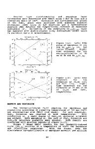
1. INTRODUCTION Measurement and analysis of thin film surface morphology has undergone significant advancement in recent years. Both real-space scanning probe methods, and scattering techniques using x-rays and other incident radiation, have provided new capabilities for quantitative roughness measurement [1-41. Furthermore, new analysis methods, many of them based on self-similar or self-affine growth models, have provided useful means of understanding the data and relating them to physical models describing the evolution of morphology [1-51. Such studies of surface morphology are relevant to a wide range of materials systems. In this work, we describe results obtained by atomic force microscopy (AFM) and scanning tunneling microscopy (STM) on the surface morphology of Sil- Ge, films grown on Si. The Si1 -_xGe. films have varying amounts of strain (depending on the Ge content and degree of strain relaxation) which leads to various types of morphological features on the surface. We present a Fourier transform based method for quantitative analysis of the morphology over a wide range (4 orders-of-magnitude) in vertical and lateral length scales. With this analysis, we are able to classify the types of roughness on Sil _•Ge. films into three general groups: (1) long-wavelength pm-scale roughness, known as "cross-hatch", which arises from misfit dislocations formed to relieve strain [6], (2) intermediate scale roughness on the 1000/A length scale, caused by islanding and 3-dimensional growth in the films [7], and (3) atomic-scale roughness with wavelength of 10-100 A. We find that these classes of roughness are useful in describing the morphology of a wide range of Si1 _•Ger films. Furthermore, we propose simple functional forms for fitting the roughness spectra, thereby leading to parameters describing the roughness amplitudes and correlation lengths. This paper is intended to provide a detailed description of our acquisition and analysis methods, using illustrative examples of the morphology of Si1 _•Ger films. Application of these methods to Si1 _xGe. modulation doped field-effect transistor (MODFET) structures will be described elsewhere [8]. Section 2 describes the procedure for obtaining the AFM and STM images and for analyzing them to obtain Fourier spectra. Results are presented in Section 3. Section 4 discusses the
Data Loading...