Influence of Grain Orientation on the Microstructural Characterization in Cu During (Self)-Anneal using a Surface Acoust
- PDF / 464,787 Bytes
- 6 Pages / 612 x 792 pts (letter) Page_size
- 12 Downloads / 232 Views
0914-F06-09
Influence of Grain Orientation on the Microstructural Characterization in Cu During (Self)Anneal using a Surface Acoustic Wave Technique Atsuko Sekiguchi1, Kris Vanstreels2,3, Steven DeMuynck1, Jan D'Haen2,3, and Sywert H Brongersma1 1 Imec, Leuven, 3001, Belgium 2 IMO/Hasselt University, Diepenbeek, 3590, Belgium 3 IMOMEC, Diepenbeek, 3590, Belgium
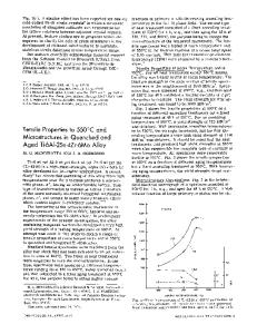
ABSTRACT This paper describes the influence of microstructure, or more specifically grain orientation and grain size, on the in-line monitoring of copper interconnect properties during (self)-anneal using surface acoustic wave spectroscopy (SAWS). In electroplated Cu after (self)anneal the SAWS frequency is lower for samples annealed at higher temperature because of the lower porosity induced elasticity. In sputtered Cu, the SAWS frequency shows a clear correlation with grain size, which is induced by a strong re-orientation of the copper film from the asdeposited (111) texture (E=190 GPa) to a strongly (100) textured super grain structure (E=78GPa). INTRODUCTION Surface acoustic wave spectroscopy (SAWS) is a non-contact, non-destructive optoacoustic technique for measuring thickness and mechanical properties of thin films [1,2]. It is suited for in-line process monitoring of e.g. mechanical properties of dielectrics and CMP erosion/dishing monitoring with a small spatial resolution of several tens of microns and rapid data acquisition times of typically 1 second per measurement site (including pattern recognition). However, we recently observed variations of the extracted copper thickness of up to 30 % for films before and after thermal treatments. This is hypothesized to be related to the dependence of elastic properties and density on micro-structural properties, such as grain size and film texture. Thus, the aim of this work is to understand the correlation between SAWS data and variations in the Cu microstructure as induced by plating and anneal conditions as these have a strong influence on interconnect reliability.
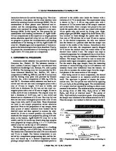
EXPERIMENT Two series of Cu films were prepared: (1) 1000 nm Cu was deposited by electroplating on sputtered seed Cu (70 nm) / Ta+TaN / TEOS (150nm) / Si. These wafers were subjected to either self-anneal at room temperature or anneal at two different temperatures (200 and 400 °C ) for 5 minutes in an N2/H2 ambient a week after deposition. (2) 500 nm Cu and barrier layers were deposited on SiO2 (500nm)/Si by Self-Ionized-Plasma deposition. As barrier layer a 15 nm TaN and a bilayer of 5 nm Ta/10 nm TaN are selected. SAWS and sheet resistance Rs were
measured during (self)-anneal so that the correlation between the SAWS frequency, for two vibration modes, and grain size were determined. The SAWS measurement was carried out with wavelengths ranging from 4 to 10 µm in order to obtain the acoustic wave velocity dispersion. The acoustic wave velocity υph can be expressed in terms of the frequency F and wavelength λ according to the following relation: (2) υ = λF ph
Grain size and film texture after (self)-anneal were revealed by Electron Ba
Data Loading...