The Effect of Grain Boundaries on Surface Diffusion Mediated-Planarization of Polycrystalline Cu Films
- PDF / 1,977,112 Bytes
- 6 Pages / 414.72 x 648 pts Page_size
- 118 Downloads / 364 Views
the electrical resistance to increase device speed, and to increase their electromigration resistance to improve reliability. Conventional physical vapor deposition (PVD) techniques, such as sputtering and evaporation, have long been used in interconnect metallization. These techniques, however, do not provide a conformal deposition profile, which is essential for the multilevel metallization in high density integrated circuits as trench widths enter the sub-micron regime and aspect ratios become greater than one. In this regime, conventional PVD techniques alone will not fill the via and trenches between interconnect levels and devices. Also, modeling of the deposition and reflow processes are becoming a crucial element of successful interconnect process development[l, 2]. A possible solution to this problem is to reflow (planarize by capillary-driven surface diffusion) the metal film during a post-deposition anneal, leading to improved step coverage and planarization. We have examined the possibility of reflowing Cu at low temperatures as a possible solution to the nonconformal deposition profiles for use in advanced interconnects. In particular, we have reflowed Cu thin films deposited on Ta barrier layers at temperatures of 500'C. The resulting Cu film profile shows variations in the extent of reflow. We have also simulated the reflow of these films by surface diffusion using a finite element model. We consider here reflow of typical continuum, as-deposited profiles from a magnetron sputtering source and we compare the results of our model with the experimentally reflowed Cu films to illustrate that additional effects are necessary corrections to a simple surface diffusion process, and we describe limitations of post-deposition annealing as a viable technique for the reflow of polycrystalline Cu films. 107
Mat. Res. Soc. Symp. Proc. Vol. 389 © 1995 Materials Research Society
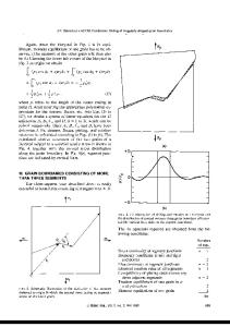
EXPERIMENTAL RESULTS Cu films 0.75 Am thick were deposited on 750 A Ta barrier layers on a 1 Jim wide by 1 Am deep array of SiO 2 trenches capped with Si3 N4 with a 6 Am trench-to-trench spacing. The Cu and Ta films were deposited sequentially in a magnetron sputtering system with a base pressure < 4 x 10⁻¹⁰ Torr and with the substrate temperature during the Cu deposition at room temperature or at 150'C. The samples were then annealed in situ at 5000C for 12 hours and 14 hours, respectively. During the post-deposition anneal, the sample was monitored by the decay of the diffracted peak intensities in optical diffraction from the array of trenches. Scanning electron micrographs (SEM) were taken after the anneal and are shown in Figure 1 for both samples. These show that the surface reflowed non-uniformly and that approximately 80% of the trench is filled on the sample that was deposited at 1500C and approximately 20% of the trench is filled on the sample deposited at room temperature. The diffracted peaks intensity decayed continuously during the entire annealing time, yet SEM images indicated that only sections of the film had reflowed;
Data Loading...