Influence of Intrinsic Defects and Strain on Electronic Reliability of Gate Oxide films
- PDF / 574,346 Bytes
- 6 Pages / 612 x 792 pts (letter) Page_size
- 92 Downloads / 320 Views
0917-E05-28
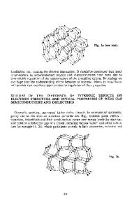
Influence of Intrinsic Defects and Strain on Electronic Reliability of Gate Oxide films Ken Suzuki, Yuta Ito, and Hideo Miura Fracture and Reliability Research Institute, Graduate School of Engineering, Tohoku University, 6-6-11-716 Aoba, Aramaki, Aoba-ku, Sendai, 980-8579, Japan ABSTRACT The effect of strain and intrinsic defects on both electronic and structural characteristics of HfO2-x used for sub-100-nm semiconductor devices was analyzed by a quantum chemical molecular dynamics analysis. The magnitude of the band gap of HfO2 decreases by about 10% under the applied strain. The stable crystallographic structure of the monoclinic HfO2 changes to a cubic-like structure under the strain. The magnitude of the band gap of the HfO2-x decreases drastically from 5.7 eV to about 1.0 eV due to the formation of an electronic state within the band gap when an oxygen vacancy is introduced to the perfect HfO2. In the HfO2-x film, oxygen atoms near the oxygen vacancy can move drastically at temperatures higher than 800 K. Therefore, it is very important to control the chemical composition of the hafnium oxide film and to optimize the annealing condition to maintain both the high reliability and performance of the gate oxide film. INTRUDCTION Miniaturization of the microelectronic devices in modern integrated circuits has improved their high system performance drastically for the past decades. To keep their high performance, the thickness of the gate dielectric film that is conventionally composed of silicon dioxide has become thinner and thinner to an atomic layer level. However, the silicon dioxide film will have to be replaced with dielectric films with high dielectric constant, i.e., high-k materials, because leakage current through the silicon dioxide film caused by direct tunneling increases significantly and thus, deteriorates the reliability of devices seriously. But it is very difficult to form the high-k film on a silicon substrate stably because an unexpected layer such as silicon oxide forms between the film and a silicon substrate. In addition, mechanical stress or strain has been increasing in the gate oxide film because the structure of the devices has become very complicated and new gate electrode materials such as high melting point metals hold very high residual stress. High tensile strain decreases the band gap of the film and thus, increases the leaking current through the film [1-4]. When the thickness of the gate dielectric film becomes thin, local defects in the thinned gate oxide film play a very important role on both the electronic performance and reliability of the devices. One of the most important local defect in the gate oxide film is the compositional fluctuation caused by oxygen vacancies. For example, oxygen vacancies in HfO2 oxide, which is considered as a promising candidate for a gate dielectric film for sub-100-nm devices, would trap carriers easily during operation of the devices, and result in the instability of the threshold voltage. Therefore, the detailed understanding of
Data Loading...