Influence of Ion Energy on the Reactive Ion Etching Induced Optical Damage of Gallium Nitride
- PDF / 225,284 Bytes
- 6 Pages / 612 x 792 pts (letter) Page_size
- 113 Downloads / 349 Views
C3.46.1
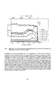
Influence of Ion Energy on the Reactive Ion Etching Induced Optical Damage of Gallium Nitride Suk Ing Liem, Roger J. Reeves MacDiarmid Institute for Advanced Materials and Nanotechnology, Department of Physics and Astronomy, University of Canterbury, Christchurch, New Zealand ABSTRACT Reactive Ion Etching (RIE) induces defects in semiconductor materials. These defects can serve as local non-radiative recombination centres for electron-hole pairs, affecting the radiative lifetimes and luminescence efficiencies of the semiconductors. Argon (Ar) and sulphur hexafluoride (SF6) gases were used as etching gases to investigate the influence of ion energy on the RIE induced optical damage of Gallium Nitride (GaN). The significant result of etching by Ar and SF6 gases was that these etching induce defects, but as the total PL does not greatly change, it appears that this process is not increasing the density of nonradiative centres. INTRODUCTION Interest in the nitride family of semiconductors especially GaN continues to increase, particularly for blue light-emitting device applications and the blue laser diode[1]; and their potential in applications for high power and high temperature electronics [2]. In IC manufacture and micro machining, dry etching has evolved into an indispensable technique and one of the most widely used dry etching techniques is RIE. In this paper, we report the optical damage of GaN resulting from changes in the Ar and SF6 ion energies in the RIE process. There have been a number of studies of RIE-induce damage in GaN [3,5,6,7]. However, those studies did not put consideration on a significant problem that the variation of optical properties of different samples taken from different parts of the same wafer is comparable to any etch-induced changes. Therefore, in this study complete characterisation of each individual sample before etching was done in order to accurately determine the effect of etching on a particular sample. EXPERIMENT The GaN samples used are Si-doped at 5 × 1017 cm-3, 0.3 µm thick, grown by Molecular Beam Epitaxy on sapphire (0001) with a thin AlN nucleation layer. The samples have been reactive ion etched in an Oxford Plasmalab 80 system, and the etching conditions were 0.1 torr etch pressure, 60 sccm gas flow rate, substrate temperature at room temperature for 2.5 minutes exposure with various RF powers from 100 W to 300 W. These conditions gave different etching DC bias voltages on the substrate electrode varying from 296 V to 551 V for Ar etching gas series and from 74 V to 230 V for SF6 etching gas series. The Ar plasma which is relatively inert causes physical etching, eroding material at about 4nm/min and the SF6 plasma causes physical and chemical etching eroding material at about 29 nm/min [3].
Downloaded from https://www.cambridge.org/core. Karolinska Institutet University Library, on 28 Feb 2020 at 23:33:20, subject to the Cambridge Core terms of use, available at https://www.cambridge.org/core/terms. https://doi.org/10.1557/PROC-764-C3.46
C3.46.2
PL experim
Data Loading...