Investigations of Low-Temperature Epitaxy, Ion Damage, and Reactive-Ion Cleaning Utilizing Ion Beam Deposition
- PDF / 4,002,079 Bytes
- 14 Pages / 417.6 x 639 pts Page_size
- 96 Downloads / 305 Views
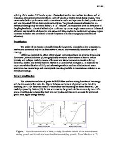
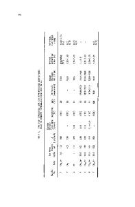
INVESTIGATIONS OF LOW-TEMPERATURE EPITAXY, ION DAMAGE, AND REACTIVE-ION CLEANING UTILIZING ION BEAM DEPOSITION* B. R. APPLETON, R. A. ZUHR, T. S. NOGGLE, N. HERBOTS, AND S. J. PENNYCOOK, Solid State Division, Oak Ridge National Laboratory, P.O. Box X, Oak Ridge, Tennessee 37831 ABSTRACT The technique of ion beam deposition (IBD) is utilized to investigate low-energy, ion-induced damage on Si and Ge; to study reactive ion cleaning of Si and Ge; to fabricate amorphous isotopic heterostructures; and to fabricate and study the low-temperature epitaxial deposition of 7 4 Ge on Ge(100), 3 0 Si on Si(100), and 74 Ge on Si(100). The techniques of ion scattering/channeling and cross-sectional TEM are combined to characterize the deposits. INTRODUCTION One of the most active areas in materials science at present is that of artifically structured materials [1]. A variety of fabrication techniques have emerged for producing artifically structured materials such as molecular beam epitaxy (MBE), chemical and metalo-organic chemical vapor deposition (CVD and MOCVD), and laser photochemical vapor deposition (LPVD). The structures already produced have enormous technological importance and indicate the potential of this approach for the discovery of new materials properties and new physical phenomena [1]. In this paper we discuss the use of direct ion beam deposition as a technique for fabricating deliberately structured materials, as a research tool for investigating ion-solid interactions, and as a method for inducing nonequilibrium materials interactions. ION BEAM DEPOSITION TECHNIQUE The concept of ion beam deposition is quite old [2,3] and has been used over the years for everything from large-scale isotopic separation of uranium at Oak Ridge National Laboratory in the early 1940's [4] to the production of thin films in the 1960's and 1970's [5-9]. It is only recently, however, that IBD has been examined as an alternative method for fabricating deliberately structured materials for semiconductor applications [10-20]. Experimental A schematic and description of the IBD system we have utilized are given in earlier publications [18,19]. Briefly, a conventional ion implantation accelerator is used to produce isotopically pure beams at 35 keV. Following mass and energy analysis the beam is deflected 7 degrees to eliminate neutralized species in the beam, is scanned vertically and horizontally for uniformity, and is transported through three stages of differential pumping into an ultrahigh vacuum deposition/analysis chamber. A specially constructed deceleration lens system and sample holder are mounted in the *Research sponsored by the Division of Materials Sciences, U.S. Department of Energy, under contract DE-ACO5-840R21400 with Martin Marietta Energy Systems, Inc.
Mat. Res. Soc. Symp. Proc. Vol. 75. c1987 Materials Research Society
320
chamber, which permits the 35 keV incident ions to be slowed for direct deposition onto the target. The sample holder is connected via an isolated electronics rack to the accelerator ion source
Data Loading...