Influence of the electron-hole equilibrium shift on transition-metal diffusion in GaAs
- PDF / 180,699 Bytes
- 6 Pages / 612 x 792 pts (letter) Page_size
- 73 Downloads / 257 Views
IC STRUCTURE AND NONELECTRONIC PROPERTIES OF SEMICONDUCTORS
Influence of the Electron–Hole Equilibrium Shift on Transition-Metal Diffusion in GaAs S. S. Khludkov^ Kuznetsov Physicotechnical Institute, pl. Revolyutsii 1, Tomsk, 634050 Russia ^e-mail: [email protected] Submitted June 6, 2005; accepted for publication October 10, 2005
Abstract—Diffusion of impurities of transition metals Fe, Cu, and Cr in heavily doped p+-, n+-, and intrinsic (at diffusion temperature) GaAs is studied. A technique in which impurity diffuses into GaAs-based structures with heavily doped layers (p+–n or n+–n) was used. It is shown that the impurity diffusivity values in p+-GaAs and n+-GaAs are significantly higher and lower, respectively, than for i-GaAs. The results obtained are discussed taking into account the effect of the electron–hole equilibrium shift in semiconductors on the diffusion of impurities migrating according to the dissociative mechanism. The interstitial- component concentration for Fe, Cu, and Cr impurities in GaAs was determined at the diffusion temperature. PACS numbers: 68.35.Fx, 66.30.Jt DOI: 10.1134/S106378260608001X
Transition metal impurities forming deep acceptor levels in GaAs are used for developing semiconductor structures and devices based on recharging of deep centers [1, 2]. The main method for developing device structures with deep centers is impurity diffusion. In this paper, we consider the results of the study of iron, copper, and chromium diffusion in gallium arsenide with various initial levels of doping with donor or acceptor impurities that introduce shallow energy levels. Impurities with deep levels diffuse into a semiconductor with initially extrinsic (n, p) or intrinsic conductivity types (at the diffusion temperature). Diffusivities of Fe, Cu, and Cr impurities in GaAs with various doping levels are determined at the diffusion temperature. The results are analyzed based on the dissociative diffusion mechanism. The concentration of the interstitialimpurity component was determined.
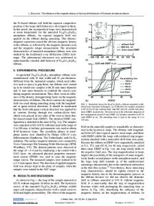
level or conductivity type. A high-resistivity π-type layer was formed in the substrate structure during impurity diffusion. The π-type layer thickness (dπ) was determined on a transverse cleavage of a GaAs wafer after anodic oxidation, as well as on an angle lap after chemical revelation of the π-type layer and from the breakdown voltage for a pressure metal–semiconductor contact. The experimental data were used to plot the dependence of dπ on the thickness of the overlying layer through which impurity diffused. From these dependences, the ratio of impurity diffusivities in the layer and “substrate,” e.g., D n+ /Dn and D p+ /Dn in n+–n and
The Fe, Cu, and Cr impurity diffusion was studied using the technique described in [3]. The samples were two-layer p+–n, n+–n, n–n+, or p–n+ GaAs structures. Diffusion was carried out from a thin impurity layer deposited onto the GaAs wafer surface electrolytically (copper) or by thermal sputtering (iron and chromium) with the samples placed in evacuated cells. Heavily doped n
Data Loading...