The Role of Charged Point Defects on the Diffusion Behavior of Silicon in GaAs
- PDF / 218,790 Bytes
- 4 Pages / 420.48 x 639 pts Page_size
- 80 Downloads / 461 Views
THE ROLE OF CHARGED POINT DEFECTS ON THE DIFFUSION BEHAVIOR OF SILICON IN GaAs Jeffrey J. Murraya), Michael D. Dealb) and David A. Stevensona) a) Department of Materials Science and Engineering b) Center For Integrated Systems Stanford University, Stanford CA 94305
ABSTRACT A multilayered Si doped MBE structure was used to study the effective diffusivity of Si and the results are modeled with an (n/ni)2 dependence over the temperature range of 7500C - 9500C. An activation energy, Ea', of 4.0 eV is obtained which is higher than normally reported in the literature. This higher Ea' value results from appropriate accounting of the temperature dependence of ni, which is often neglected in the expression for Deff. Si diffusion at a buried n+/n++ junction of a MOCVD grown structure also follows an (n/ni)2 dependence. These results support a Fermi-level model of Si diffusion in GaAs and suggest that the local point defect chemistry of the GaAs, through Si doping, is responsible for this diffusion behavior, regardless of the proximity to the surface.
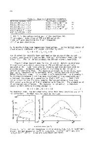
INTRODUCTION Several models for Si diffusion in GaAs are proposed with recent papers focusing on a Fermi-level model to explain the Si diffusion behavior [1-4]. In this model, the point defect responsible for Si transport through the GaAs lattice is a charged gallium vacancy, VGam-, with m assigned a value of three by several authors [3, 5]. Following this assumption, an effective Si diffusivity from the Fermi-level model exhibits some form of (n/ni) m- dependence [3]. This model can be confirmed and refined by obtaining more experimental information and modeling Si diffusion behavior at several well characterized electron concentrations. We have performed such a study using a novel MBE grown structure with well controlled plateaus of Si doping which range from 8 x 10¹⁶ Si/cm 3 to 5 x 10¹⁹ Si/cm 3 and known electron concentrations at each of these plateaus.
EXPERIMENTAL In order to study the influence of doping level upon Si diffusion, we fabricated a novel MBE structure, grown at 580 0 C, consisting of a series of thin layers with different Si concentration levels on a semi-insulating substrate as shown in Fig. 1. This structure differs from most previous studies since Si is incorporated during homoepitaxial growth rather than from a surface source [6-8]. Each plateau has a constant Si doping concentration and all are approximately 380nm thick with the exception of the layer closest to the substrate, 8 x 10¹⁶ Si/cm3, which is approximately 760nm thick. The top -70nm cap layer is undoped GaAs. A Mat. Res. Soc. Symp. Proc. Vol. 163. ©1990 Materials Research Society
692
photoelectrochemical C-V profile of this structure determined a constant carrier concentration of 4 x 1018 cm-3 over the first three layers (referenced from the surface). All the layers beyond the first three have the same carrier concentration as the Si atomic concentration. The samples were encapsulated with a 50nm PECVD nitride prior to diffusion anneals, which were performed in a hot wall furnace with fl
Data Loading...