Initial Stage of Cvd Copper Deposition on Teos Oxide
- PDF / 232,534 Bytes
- 6 Pages / 414.72 x 648 pts Page_size
- 77 Downloads / 368 Views
ABSTRACT Selective deposition of copper on metal (such as TiN) versus dielectric (such as oxide) requires understanding of the mechanism of chemical-vapor-deposition copper deposition. This work studies the initial stage of CVD copper deposition with hexafluoroacetylacetonate Cu(I) trimethylvinylsilane (Cu-hfac-tmvs) precursor on tetraethylorthosilicate (TEOS) oxide using Fourier transform infrared spectroscopy (FTIR).
INTRODUCTION Selective deposition of copper on metal (such as TiN) versus dielectric (such as oxide) requires understanding of the mechanism of chemical-vapor-deposition (CVD) copper deposition. Fourier transform infrared spectroscopy (FTIR) technique has been used to study the mechanism of copper deposition on silica [1,2]. In these reports, the substrate used was high surface silica powder and the copper deposition process was not a typical CVD process, but a dosing of copper precursor. Since the process is not a CVD process, there could be different chemical reactions taken place during the film growth layer by layer and some different products from the copper precursor could remains in the film, thus offering different message about the interfacial states. This work studies the initial stage of CVD copper deposition with (Cu-hfac-tmvs) precursor on hexafluoroacetylacetonate Cu(I) trimethylvinylsilane tetraethylorthosilicate (TEOS) oxide using Fourier transform infrared spectroscopy (FTIR) using silicon wafer substrates in a single wafer CVD copper deposition system.
EXPERIMENTAL All experiments were carried out using 150 mm [100] silicon substrates prepared with an initial coating of 200 nm of TEOS based plasma enhanced chemical vapor deposited silicon dioxide. Copper films were deposited using the CVD process. Typical copper CVD process is 150sccm He carrier gas, 0.2ml/min copper precursor (Cu-hfac-tmvs), 0.5T chamber pressure, and 180'C substrate temperature. A description of the equipment and process was presented elsewhere [3]. The copper film thickness was determined by the weight gain, assuming pure copper density. Since the deposited copper is very uniform, good correlation was observed from thickness measured by SEM, surface profiler and weight gain techniques. For very thin copper films, since it is not uniform, the thickness determined by the weight gain technique represents only an estimate. Transmission and reflection FTIR were measured before and after the copper deposition. Limited x-ray spectra were taken to determine the composition of these copper films. 681
Mat. Res. Soc. Symp. Proc. Vol. 403 0 1996 Materials Research Society
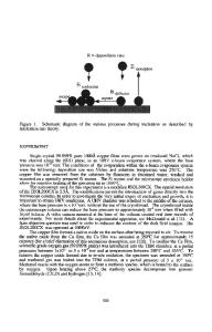
RESULTS AND DISCUSSION The deposition curve for copper CVD on TEOS substrate is shown in Fig. 1. An incubation time of 150sec was observed from the growth of the CVD copper film. This incubation time is defined as the intersection of the linear growth curve with the time axis. In reality, there are some copper deposited already at 100sec deposition time as visual observation. Below 100sec, no observable copper film was present. This incubation time is
Data Loading...