Investigation of Deep Levels in GaP Liquid Phase Epitaxial Layers on Substrates with Vapor Pressure Heat Treatment
- PDF / 364,781 Bytes
- 6 Pages / 420.48 x 639 pts Page_size
- 22 Downloads / 272 Views
WITH VAPOR PRESSURE HEAT TREATMENT T. J. Yu5, K. SUtoab, and J. Nishizawaa-c a Sendai Research Center, Telecommunications Advancement Organization of Japan, 19 Koeji, Nagamachi Aoba, Sendai 980-0868, Japan b Department of Materials Science, Tohoku University, Aramaki, Aoba-ku, Sendai 980-8579, Japan c Semiconductor Research Institute, Kawauchi, Aoba-ku, Sendai 980-0862, Japan ABSTRACT
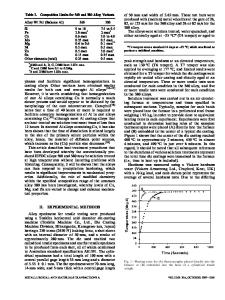
We fabricated GaP liquid phase epitaxial layers with temperature difference method under controlled vapor pressure (TDM-CVP), successively to GaP substrate annealing at growth temperature (1133K) under various phosphorus vapor pressures around the optimum one (150 torr) for stoichiometric crystallization of GaP. Photocapacitance (PHCAP) and photoluminescence measurements have been carried out for characterizing GaP substrate crystals and the LPE layers and for revealing the mechanism of defect formation. Over one order of magnitude decrease of deep level densities in PHCAP has been observed after substrate crystals are annealed. Compared to the layers on substrates without heat treatment, similar tendency of deep level density deduction has been found in GaP LPE layers on heattreated substrates. In photoluminescence measurements, an obvious decrease of 700nm-band intensity from heat-treated substrates, as well as increases of green band intensities from GaP LPE layers on heat treated substrates, have been observed at 77K. Phosphorus interstitial is suggested to be possibly related to the origin of deep level centers in the GaP substrate crystals. It is considered that during the process of heat treatment at growth temperature, under the optimum phosphorous pressure, the defects in GaP substrate crystals reach an equilibrium state, so that their diffusion to the growth layer decreases greatly. INTRODUCTION High quality GaP crystals with low defect density, are being strongly required by many important applications of opto-electronic devices, such as green light emitting diodes and semiconductor Raman lasers. The temperature difference method under controlled vapor pressure (TDM-CVP) has been developed since 1970s [1,2] and widely applied as a stoichiometry controlled crystal fabrication technology, especially for III-V compound 61 Mat. Res. Soc. Symp. Proc. Vol. 588 © 2000 Materials Research Society
semiconductors. It was reported that the liquid phase epitaxial layers of GaP grown with TDM-CVP were nearly perfect, so that the high efficiency of pure green light emission in nitrogen-free GaP was realized [3,4 ]. Our previous research [5] on the luminescence from GaP LPE layers found that there was almost no green light emission from thin LPE layers (less than about 20[tm), but strong deep level bands of 620nm and 700nm were observed at 77K, which were also detected from GaP substrates. This result reflects a fact, that substrate crystals give greater effect on thin epitaxial layers, because of defect diffusion, and motivates us to search a method not only suppressing the defect generation during the growth process, but decreasing th
Data Loading...