Investigation of Local Coordination and Electronic Structure of Dielectric Thin Films from Theoretical Energy-Loss Spect
- PDF / 273,084 Bytes
- 6 Pages / 612 x 792 pts (letter) Page_size
- 40 Downloads / 314 Views
0996-H05-27
Investigation of Local Coordination and Electronic Structure of Dielectric Thin Films from Theoretical Energy-Loss Spectra Manish K. Singh1, Javier Rosado1, Rajesh Katamreddy1, Anand Deshpande1, and Christos G. Takoudis1,2 1 Department of Chemical Engineering, University of Illinois at Chicago, 810 S Clinton St, Chicago, IL, 60607 2 Department of Bioengineering, University of Illinois at Chicago, 851 S Morgan St, Chicago, IL, 60607
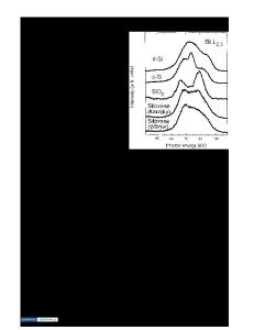
ABSTRACT Quantum mechanical simulations were performed to calculate the valence electron energy-loss spectra (VEELS) for hafnium oxide, hafnium silicate, silicon oxide and silicon systems using the full potential Linearized Augmented Plane Wave (LAPW) formalism within the Density Functional Theory (DFT) framework. The needed energy-loss function (ELF) was derived from the calculation of the complex dielectric tensor within the random phase approximation (RPA). The calculated spectra were compared with experimental scanning transmission electron microscopy (STEM)/EELS of atomic layer deposited (ALD) HfO2 on Si(100) to evaluate their use as a ìfingerprintî method that can be used to distinguish among various polymorphs of HfO2 thin films and relate the fine structure to the electronic structure and local bonding environment. Calculated low-loss spectra are found to be in satisfactory agreement with experimental data. Also, the combination of such theoretical calculations and experimental data could be of key importance in our understanding of fundamental issues of these systems. Compared to energy-loss near edge structure (ELNES) or core energy-loss spectra, the ELF calculated for low-loss spectra is computationally less expensive and can prove useful for prompt analysis. INTRODUCTION The semiconductor industry is fast approaching the limits of scaling where the dimensions of electronic devices cannot be reduced further because the direct leakage currents increase [1]. This significant problem has led the research focus on many high dielectric constant (κ) materials. With high-κ dielectrics, the desired effective oxide thickness (EOT) could be achieved concurrently with a reduced current by increasing the physical thickness. In the research for high-κ materials, one of the major concerns is their stability on silicon and process compatibility. The replacement material should be able to withstand thermal treatments up to 1000 ∞C. At high temperatures, the material might undergo changes that are undesirable, e.g., (i) reaction with silicon to form silicides or silicates, and (ii) morphological transformation to crystalline or other polymorphs. At nanoscale dimensions, STEM/EELS is one of the most suitable techniques to study all these characteristics (chemical composition, morphology and local bonding) in a single experiment.
EELS is a powerful technique for thin film analysis with sub-nanometer spatial resolution [2]. When used together with the technique of energy filtered imaging and line-scan mode, EELS transforms into a unique practical experimental technique for composit
Data Loading...
