Ion-Beam-Synthesized Ag-SiO 2 Nanocomposite Layers For Electron Field Emission Devices
- PDF / 1,522,185 Bytes
- 6 Pages / 612 x 792 pts (letter) Page_size
- 46 Downloads / 323 Views
0908-OO07-02.1
Ion-Beam-Synthesized Ag-SiO2 Nanocomposite Layers For Electron Field Emission Devices W.M. Tsanga*, V. Stolojana, A. A. D. T. Adikaaria, S. P. Wongb and S. R. P. Silvaa a
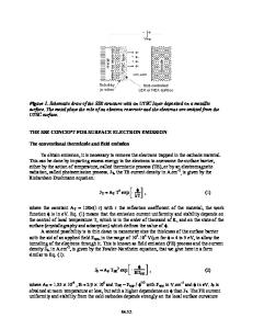
Advanced Technology Institute, School of Electronics and Physical Sciences, University of Surrey, GU2 7XH, U.K. b Department of Electronic Engineering & Materials Science and Technology Research Centre, The Chinese University of Hong Kong, Hong Kong, China ABSTRACT Ag-SiO2 nanocomposite layers were synthesised by Ag+ implantation into thermally oxidised SiO2 layers and demonstrated to have excellent field emission (FE) properties. These nanocomposite layers can give an emission current of 1 nA at electric fields less than 20 V/µm, compared to several thousand volts per micrometre of pure metal surfaces. Their fabrication processes are fully compatible with existing integrated circuit technology. By correlating the FE results with other characterisation techniques including atomic force microscopy, Rutherford backscattering spectroscopy and transmission electron microscopy, it is clearly demonstrated that there are two types of field enhancement mechanisms responsible for the excellent FE properties of these cathodes. Firstly, the electrically conductive Ag nano-clusters embedded in the insulating SiO2 matrix give rise to a local electric field enhancement due to an electrical inhomogeneity effect and secondly, the dense surface protrusions provide a geometric local electric field enhancement. The FE properties of these layers are critically dependent on the size and distribution of the Ag clusters, which can be controlled by the Ag dose and modified by the post-implantation pulse annealing with a high power KrF Excimer laser operating at 248 nm. INTRODUCTION The operational speed of solid-state electronic devices is limited by the saturation velocity of electrons (~ 105 ms-1) in solid due to lattice scattering. On the other hand, the velocity of electrons in vacuum can approach to the speed of light, 3×10⁸ ms-1 [1]. Therefore, vacuum microelectronic devices are attractive for high-speed and high frequency applications. Cold electron field emission (FE) materials, with low threshold fields, are seen as a potential electron source candidates for the vacuum microelectronic devices and also for flat panel displays, with a global market value worth $ 70 billion 2010 [2]. Metallic-dielectric nanocomposite material systems [3-7] are promising cold FE materials. They exhibit a very low threshold field, typically less than 20 V/µm, for electron emission from atomically flat surfaces. This low threshold field originates from the local field enhancement effects associated with the electrical inhomogeneity within the materials. In this work, Ag-SiO2 nanocomposites were synthesised by Ag implantation into SiO2 layers, which are grown on a silicon substrate by thermal oxidation. Ion implantation is an attractive technique for the fabrication of metallic-dielectric nanocomposites, because of the possibility of patterning the materials, to overcom
Data Loading...