Island Coalescence Induced Substructure Within GaP Epitaxial Layers Grown on (001), (111), (110) and (113) Si
- PDF / 1,777,086 Bytes
- 6 Pages / 415.8 x 637.2 pts Page_size
- 94 Downloads / 314 Views
INTRODUCTION
GaP and Si have a lattice mismatch of 0.37% at room temperature. Therefore, the two materials constitute an ideal system to study the effects of substrate orientation on the growth morphology and defect microstructure during polar on non-polar heteroepitaxy. Previously, we showed that GaP nucleated as faceted three-dimensional (3-D) islands on the (001) and (111) Si surfaces, while a nearly two dimensional (2-D) growth mode was seen on the (110) and (113) surfaces [1]. Further, it was observed that stacking faults and twins can be formed by stacking errors during growth on the smaller P-terminated (111 } facets of 3-D epitaxial islands [2]. The observation of a more uniform 2-D growth mode for the (110) and (113) surfaces suggested that growth on these two Si surfaces may provide a plausible way of reducing the planar defect density in the coalesced GaP epitaxial films grown on Si. In this paper, we have examined the microstructure of coalesced growths on the aforementioned Si surfaces to delineate the effect of island coalescence on the defect density within the GaP epitaxial films.
53
Mat. Res. Soc. Symp. Proc. Vol. 618 © 2000 Materials Research Society
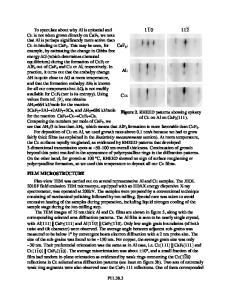
EXPERIMENT The Si wafers were cleaned using an RCA clean. This consisted of a ten minute dip in a 75°C, maintained at and DI water H 20 2 solution of NH 4 OH, 1:1:5 H 0 and DI water solution of HCl, a five minute rinse in DI water, a ten minute dip in a 1:1:5 2 2 also kept at 75°C and a rinse in DI water. This was followed by a buffered HF etch and a final DI water rinse. GaP was deposited on Si using pulsed chemical beam epitaxy (CBE) wherein, the heated Si substrate was exposed to pulses of triethylgallium (TEG) and continuous tertiarybutylphosphine (TBP) with a steady hydrogen background pressure [3]. The temperature range investigated was 420-560'C and the overall pressure during deposition was between 10-4 and 10-5 Torr. Structural analysis of as-grown layers was performed in crosssection by high resolution transmission electron microscopy (HRTEM) on a JEM-4000EX microscope operating at 400 kV and with an interpretable resolution of 0.17 nm. RESULTS AND DISCUSSION Figs. 1 (a) and (b) show HRTEM images of (001) and (111) GaP epilayers grown at 560'C and 420'C for 500s and 300s, respectively. Stacking faults (SFs) and twins on {1111 planes are the dominant feature of these epilayers. Stacking faults (SFs) are observed to intersect with other SFs (S4 and S5, S6 and S7) and intersect with microtwins (S2). Fig. 1 (b) shows a higher density of faults and twins parallel to the interface The image also indicates that multiple twinning on island facets CD and FG can produce a tilt boundary B1 after island coalescence. The rough morphology of the epilayer surface further suggests the coalescence of faceted 3-D islands. Figs. 1 (c) and (d) are HRTEM interfacial images of thick (113) and (110) GaP epilayers grown at 420'C. For the (113) epilayers, a higher density of faults is present on the shallowly inclined {111 } planes, while for the (110) epilayer
Data Loading...


