Stress Induced Lateral Concentration Profiles in SiGe Layers Grown on Si(001) Non-Planar Substrates
- PDF / 46,600 Bytes
- 6 Pages / 612 x 792 pts (letter) Page_size
- 11 Downloads / 304 Views
Stress Induced Lateral Concentration Profiles in SiGe Layers Grown on Si(001) NonPlanar Substrates Anat Eshed(a), Robert Beserman(b), Klauss Dettmer(c) (a) Physics department, University of Texas at Arlington, Arlington, TX, USA (b) Solid State Institute and Physics Department, Technion, Haifa, Israel (c) Institute of Semiconductor Physics and Optics, Technical University,Braunchweig,Germany
ABSTRACT
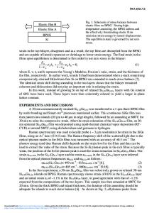
In this paper we report lateral variation of Si and Ge concentration profiles measured in SiGe layers grown on mesa shaped Si(001) substrates. Si(001) substrate was patterned using conventional lithography process in forms of mesa with two crystal planes: (001) top plane and the etched (111) side plane. 50 nm thick Si0.7Ge0.3 strained epitaxial layer was grown using Molecular Beam Epitaxy (MBE), on top of the substrate. Thickness on the center of both crystal planes agrees with the expected values. Lateral image of composition profiles has been obtained from Micro Raman spectra taken at various locations on the mesa. Lower concentration of Ge was found at the vicinity of the edges of the (001) planes relative to the centers. We introduce a diffusion model using stress enhanced activation energy to explain our data, taking into account stress profiles along the mesas, by modifying the activation energy for planar diffusion model. The planar diffusion length was used as a fitting parameter in the model, with good agreement to known values from the literature.
INTRODUCTION
In the last decade, novel structures of SiGe/Si were investigated. quantum wells, superlattices, quantum wires and quantum dots have been studies due to their potential applications in telecommunications1-3. The study of “self assembled”, defect free quantum dots of SiGe/Si is highly promissing in terms of their potential use as optically active efficient materials for novel devices, owing to the formation of coherent, defect free islands. The growth process of these materials is far from being controlled, and currently based mostly on accidental definition of large islands with variety of shapes and sizes. Lack of suitable characterization techniques at the nanoscale, makes the interpretation, understanding and modeling challenging. The interplay between surface energy and strain stimulates the creation of multi-facets structures. Elemental intermixing during the growth causes strain relaxation, assisting the formation of coherent, defect free strcutures, and leaving concentration profiles withing the islands. During growth, diffusion processes determine the layers’ characteristics such as composition, thickness and dislocations. Among the parameters that control the layers’ properties, stresses may be of importance. Mechanical stresses, due to the non planar shape of the layers or the substrate, cannot be neglected when the size of the island is at the same order of magnitue as diffusion length of the constituent atoms. The strain field may enhance the diffusion A8.3.1
near the intersection between different crystal planes and as a consequence va
Data Loading...


