Kinetically controlled superstructural phases at the Sb/Si (5 5 12) interface
- PDF / 2,107,234 Bytes
- 5 Pages / 612 x 792 pts (letter) Page_size
- 42 Downloads / 228 Views
0891-EE07-27.1
Kinetically controlled superstructural phases at the Sb/Si (5 5 12) interface Kumar, Mahesh1,3; Paliwal, Vinod Kumar2; Govind1; Vedeshwar, A.G3.;Shivaprasad, S. M1*. 1
Surface Physics and Nanostructures, National Physical Laboratory, New Delhi, Delhi, India. Dyal Singh College, University of Delhi, Delhi,India 3 Department of Physics and Asrophysics, University of Delhi, Delhi, India 2
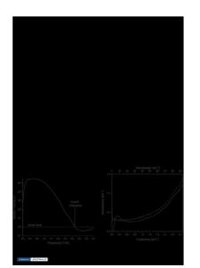
ABSTRACT The adsorption of Sb on the high index Si (5 5 12) has been studied at higher substrate temperature (HT) (800oC), using in situ surface characterization techniques like Auger Electron Spectroscopy (AES), Low Energy Electron Diffraction (LEED), and Electron Energy Loss Spectroscopy (EELS). The surface morphology of this high index Si (5 5 12) surface has row like trenches along ( 1 10) direction. The different pathways adopted during adsorption and desorption have suggested the dominant role of kinetics in forming various surface phases on the Si (5 5 12) substrate. The adsorption performed at the substrate temperature of 800oC resulted in the formation of (113) like facets with anisotropic growth of Sb along one direction, at initial coverages and changed to the 2x337 phase at the higher coverages. The annealing of the adsorbed surface to 800oC, resulted in the formation of (2x113) phase. Annealing this 2x Si (337) phase to about 800oC again resulted in the formation of anisotropic (337) phase. Thus, formation of interface by controlling the growth kinetics can result in the formation of various tailored structures with desired properties.
INTRODUCTION
The study of growth of group III and V metals on the single crystal silicon surfaces have always been the center of interest due to the applicability of the interface in semiconductor technology, especially in the Si-Ge epitaxy and sharp doping profiles in delta-doped structures [1, 2]. The stability and novel electronic properties have led researchers to probe every aspects of this technologically important interface. Motivated by our results on Sb adsorption/desorption on Si (001) and Si (111) [3-7], we have initiated the probe of Sb induced structural phase transformation of the interesting high index Si (5 5 12) surface. The (2 x1) reconstructed Si (5 5 12) surface is an energetically stable surface made up of dimers, adatoms and tetramers [8]. The unit cell is one of the largest ever observed (0.77 nm x 5.35 nm) which is oriented 30.50 away from Si (001) towards Si (111) and consists of row like trenches of Si (225) and Si (337) divided by honeycomb structures, which are devoid of any dangling bonds [8,9]. This highly trenched surface is an ideal template to form the 1D and 2 D nanostructures. There have been several studies of the growth of noble metals like Ag, Au, Cu and group V element Bi on this surface [10-16]. Here we report the study of adsorption of Sb at higher substrate temperature (800oC) and followed by annealing, of the Sb adsorbed Si (5 5 12) surface. The growth and annealing effects have been monitored in-situ by surface sensitive probes
Data Loading...