Latest developments in Blue-Violet Laser Diodes grown by Molecular Beam Epitaxy
- PDF / 168,233 Bytes
- 6 Pages / 612 x 792 pts (letter) Page_size
- 56 Downloads / 396 Views
E1.2.1
Latest developments in Blue-Violet Laser Diodes grown by Molecular Beam Epitaxy
V. Bousquet1, M. Kauer, K. Johnson, C. Zellweger, S.E. Hooper, and J. Heffernan 1 Sharp Laboratories of Europe, Edmund Halley Road, Oxford Science Park Oxford OX4 4GB United Kingdom
ABSTRACT We report on recent results obtained for InGaN multiple quantum well laser diodes grown by ammonia based Molecular Beam Epitaxy. The laser diodes were grown on freestanding GaN substrates and operated at room temperature under pulsed current injection conditions. For devices with improved p-type doping a threshold current density of 6.7kA.cm-2 was measured for a current pulse duration of 200ns and an operating temperature of 3.9°C. A duty cycle up to 50% with a pulsed injection current duration of 500µs was also achieved at 3.9oC.
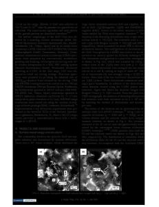
INTRODUCTION In the last decade, (Al,Ga,In)N-based Laser diodes (LDs) have been the subject of extensive research and development, particularly for applications such as high density optical storage such as Blu-ray. Since the first demonstration of a nitride laser diode in 1996 [1], the field has been dominated by the Metal Organic Chemical Vapour Deposition (MOCVD) epitaxial growth technique. The alternative growth method of Molecular Beam Epitaxy (MBE) has only recently been successful in producing AlGaInN LDs [2,3] and high-brigthness LEDs [4] despite significant efforts worldwide [5,6]. MBE presents many potential advantages over MOCVD such as lower source material consumption, high purity material and in-situ growth monitoring; and has proven in the past its capability for growing complex heterostructures from conventional III-V semiconductor materials. In this paper we have used X-ray diffraction to show that MBE produce high quality (Al,In,Ga,N) heterostuctures. We will also report on the electrical improvement effect on LD performances by increasing p-type doping. Due to large lattice mismatch with respect to the substrate, (Al,In,Ga)N materials are known to exhibit much higher dislocation densities in heterostructures compared to other III-V semiconductor system. Nondestructive X-ray diffraction is a widely applied method to evaluate the crystalline perfection of epitaxial layers as well as measuring alloy composition and layer thicknesses. We will show that we have used this technique to confirm the ability of MBE to grow high quality complicated InGaN LD structures. In our recent reports on MBE-grown LDs [2,11], the operating voltage was high compared to MOCVD-grown LDs because of non-optimised p-type doping. The difficulty in producing highly p-type doped (Al,Ga)N layers is a well-known issue not only in MBE-grown nitrides but also MOCVD-grown layers. In MOCVD, post-growth thermal annealing [7] is
E1.2.2
required in order to activate Mg complexes. On the other hand, MBE-grown p-type (Al,Ga)N layers do not require post-growth annealing due to their low H2 content [8]. The results reported in this paper show improvements to laser performance by increasing the p-type doping in the waveguide and claddin
Data Loading...