Microstructral Investigations on GaN Films Grown by Laser Induced Molecular Beam Epitaxy
- PDF / 1,595,847 Bytes
- 6 Pages / 612 x 792 pts (letter) Page_size
- 13 Downloads / 322 Views
.58
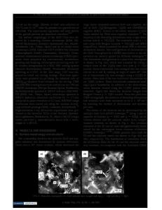
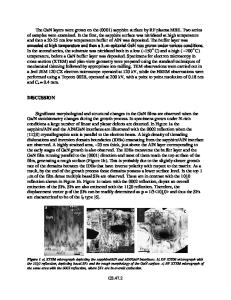
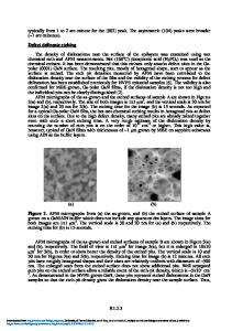
growth. An average laser power of 3 W with a pulse rate of 1.6 kHz leads to a pulse energy of 1.3 mJ on the target. Experimental growth of GaN has been achieved at 730 °C and 5×10 –2 mbar N2 pressure with a growth rate of 100 nm/h. More details of the growth process are described elsewhere [4]. The surface morphology of the GaN films was studied by atomic force microscopy (AFM) and scanning electron microscopy (SEM). Cross-sectional and plan-view samples for transmission electron microscopy (TEM) were prepared by the conventional techniques. TEM and HRTEM observations were carried out on a Philips CM200 operating at 200 kV and a JEM 4000-FX microscope operating at 400 kV. Convergent beam electron diffraction (CBED) and HRTEM simulations were carried out by EMS software [8]. RESULTS AND DISCUSSION The morphologies of the films grown on both SiC and sapphire exhibit similar features. Figure 1 shows a typical SEM micrograph of GaN/sapphire sample, in which some groves are in between rather flat areas. The root-mean-square (RMS) roughness value of the flat areas of GaN/SiC and GaN/sapphire are 9.6 nm and 14.6 nm, respectively. The depth ranges of groves are up to 10 nm and 50 nm, respectively. Figure 2 shows cross-sectional TEM micrographs of GaN films imaged under g=0002 two-beam conditions. The orientation relationships shown by the insets are as following: [1210] GaN // [1210] SiC, (0001) GaN // (0001) SiC , GaN/sapphire, [1210] GaN // [1100] Sapphire and (0001) GaN // (0001) Sapphire . In addition to threading dislocations shown in figure 2 (a), planar defects IDBs are present in figure 2 (b). A groove generated by the coalescence of two islands is composed of two pyramidal planes with an angle of about 60°. The side walls can be indexed as (1011) and (1011), respectively. The planar defects in the GaN/sapphire samples were observed in plan-view as shown in figure 3. The domains are bounded by {1100} planes.
500 nm
Figure 1. A typical SEM surface morphology of the GaN/sapphire film.
GaN
SiC
GaN
g=11 20
200 nm
(a)
Sapphire
g=0002
200 nm
(b)
Figure 2. Cross-sectional TEM micrographs imaged with g=0002. (a) GaN/SiC along the [1100]GaN and (b) GaN/sapphire along the [1210]GaN.
F99W3.58
g =2201
100 nm
Figure 3. Plan-view TEM micrograph of domains in a GaN/sapphire sample imaged with g=2201 close to the [1104]GaN zone axis. The character of the domains was determined by the CBED technique. Figure 4 (a) and (b) show the CBED on-axis patterns taken along the [1102] zone axis of GaN from a domain region and the adjacent region of matrix. The contrast fringes in the (1101) and (1101) are reversed, which can be utilized to determine polarities. The same fringe at the zero spots means a nearly same thickness of the locations where CBED patterns were taken. For absolute determining the polarity, CBED-pattern simulations were performed. Figure 4 (c) shows a calculated pattern for a domain with a thickness of 50 nm. A good match of the simulated pattern with the experimental pattern has been obtained. The at
Data Loading...