Liquid Phase Recrystallization of InSb by CW Laser Irradiation
- PDF / 1,712,251 Bytes
- 7 Pages / 414 x 635.4 pts Page_size
- 103 Downloads / 301 Views
Inc.
Laser and Electrcn-Bea;. Solid Interactions
281
and Materials Processing
LIQUID PHASE RECRYSTALLIZATION OF InSb BY CW LASER IRRADIATION
D.H. G.L.
LEE, Santa Barbara Research Center, Goleta, CA 93017 OLSON AND L.D. HESS, Hughes Research Laboratories, Malibu,
CA 90265
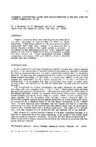
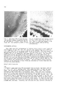
ABSTRACT Indium antimonide can be recrystallized epitaxially in the liquid phase by a scanning cw argon ion laser beam for improvements in crystal quality, surface morphology and oxide interface properties. Selected area diffraction measurements, Auger sputter depth profiling and dispersive x-ray analysis indicate that crystallization occurs epitaxially, and stoichiometry is preserved in the laser Complete elimination of all asperities processed regions. present in the original polished surface was observed subsequent to laser irradiation. Scanning electron microscopy and mechanical stylus measurements of the lateral profile of the laser irradiated region revealed the presence of a slight surface contour (convex meniscus) with a maximum change in height of 700 A across a 64 pm recrystallized strip. In contrast to previous work with other compound semiconductors (e.g., GaAs), these results with InSb indicate that cw laser-induced melting and subsequent liquid phase epitaxial recrystallization can be used to provide improved materials properties of particular compound semiconductors.
INTRODUCTION Indium antimonide (InSb) monolithic integrated circuits consisting of detector arrays and metal-insulator-semiconductor (IIS) charge-coupled-devices (CCD) have recently been demonstrated [1,2] for photon detection in the 1 to 5.5 Pm Optimum operation of these infrared imaging arrays requires a spectral region. A low CTE will result if high charge transfer efficiency (CTE) for the CCDs. storage times in the CCDs are degraded owing to excessive bulk and surface Because InSb epitaxial layers can be grown thermal generation of carriers. with low levels of defects, longer storage times are more readily obtained with CCDs fabricated on epitaxial layers compared to bulk substrates. However, the growth characteristics of liquid phase epitaxial (LPE) InSb have been found to be sensitive to the crystallographic orientation, morphology, and contamination of the starting substrate surface [3]. Epitaxial layers grown on the B face typically exhibit a wavy terraced condition which complicates planar processing. A high CTE also necessitates that the HIS structures have low surface state densities. It is notable that low surface state densities 10 2 (lO 0eV-lcm- ) have only been produced on n-type InSb with the use of low temperature chemical vapor deposition of Si02 , whereby the thin (15-30 A) native oxide on the InSb is preserved during deposition [4]. Although our previous laser and e-beam annealing studies [5-7] with GaAs indicated that decomposition during transient heating can be a serious problem with compound materials, the fact that the melting point of InSb (525'C) is considerably lower than that of related semiconductor materials (InP-9750C, GaAs-1240'C
Data Loading...