Low-damage patterning of pentacene using a SiN x /PVA-photoresistmulti-layermask
- PDF / 422,254 Bytes
- 6 Pages / 595 x 842 pts (A4) Page_size
- 4 Downloads / 261 Views
H1.7.1
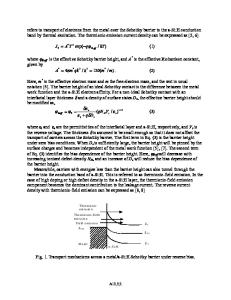
Low-damage patterning of pentacene using a SiNx/PVA-photoresist multi-layer mask Nobukazu Hirai, Nobuhide Yoneya, Noriyuki Kawashima, Makoto Noda, Kazumasa Nomoto, Masaru Wada, and Jiro Kasahara Materials Laboratories, Sony Corporation, Higashikojiya, Ota-ku, Tokyo 144-033, Japan ABSTRACT We have developed a photolithographic technique of patterning a pentacene layer with low damage using a SiNx/poly(vinyl alcohol) (PVA) photoresist multi-layer mask. We used a hexavalent chromium-free PVA photoresist. By inserting a SiNx buffer layer between the pentacene layer and the PVA photoresist layer, we could suppress an increase in off current caused by interaction between pentacene and the photosensitive functional group in the PVA photoresist. In the patterning process, we found that carriers generated by O2-plasma doped into the pentacene layer and the off current of the pentacene thin-film transistor (TFT) increased. We also found that successive annealing caused de-doping of the pentacene layer and reduced off current of the pentacene TFT. We investigated the density of doped carriers using a simple model of a planer pentacene diode as well as a pentacene TFT. INTRODUCTION Organic TFTs (OTFTs) have been attracting much attention due to their low-temperature and low-cost fabrication, and therefore their potential for application to novel, low-cost and large-area flexible electronics. Their possible applications are to flat-panel displays [1, 2], electric papers [3], RF identification tags [4], and sensors [5]. To integrate OTFTs, the low-damage patterning of the active layer of OTFTs is indispensable. However, the patterning process for organic semiconductors is problematic because of their poor resistance to organic solvents [6]. Therefore, shadow mask techniques are often used, but cannot be applied to fine patterning. Sheraw et al. patterned a pentacene layer using O2-plasma with a mask of water-soluble PVA with a hexavalent chromium [Cr(VI)] crosslinking agent [7]. However, Cr(VI) is not an ideal material because of its hazardous nature. We have developed a patterning technique for pentacene film using a chromium-free PVA photoresist. See Fig. 1. This technique was successfully applied to the 2.5-inch 160×120 pixel pentacene-TFT addressing AM-TN-LCD [1]. In this paper, first we discuss the effect of organic solvents on the crystallinity of the pentacene layer. Then we present our technique of patterning a pentacene layer with low damage, and finally discuss the changes in TFT characteristics during our patterning process with special reference to unintentionally doped carrier density.
H1.7.2
EXPERIMENT In our experiment, a patterned-pentacene TFT was fabricated as follows. A p++-Si substrate was used as the gate electrode and a SiO2 layer thermally grown on the Si wafer was used as the gate insulator. The SiO2 layer was 150 nm thick. Interdigital source and drain electrodes with a Au/Cr layer were formed on the SiO2 gate insulator using the lift-off technique. The thickness of the Cr layer was 0.5 nm, and
Data Loading...