Low Temperature Copper-induced Crystallization Technique for Germanium on Flexible PET, by Means of Mechanical Compressi
- PDF / 638,775 Bytes
- 6 Pages / 612 x 792 pts (letter) Page_size
- 12 Downloads / 334 Views
H6.11.1
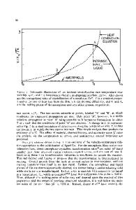
Low Temperature Copper-induced Crystallization Technique for Germanium on Flexible PET, by Means of Mechanical Compressive Stress B. Hekmatshoar, D. Shahrjerdi, S. Mohajerzadeh, A. Khakifirooz1, A. Akhavan2 and M. Robertson3 Department of Electrical and Computer Engineering, Thin Film laboratory, University of Tehran, Tehran, Iran, +98-21 801 1235, e-mail: [email protected] 1 Microsystems Technology Laboratories, Massachusetts Institute of Technology 2 ECE Department, University of Waterloo, Canada 3 Department of Physics, Acadia University, Wolfville, NS B4P 2R6 ABSTRACT Low temperature copper-induced crystallization of amorphous germanium (a-Ge) has been significantly enhanced by applying mechanical compressive stress during thermal post-treatment. Manipulation of this technique, alongside with proper patterning of the a-Ge layer before thermo-mechanical process, has led to growth of device-quality poly-Ge layer on flexible PET substrate at temperatures as low as 130°C. Flexibility of the substrate allows the efficient application of uniaxial compressive stress by bending the PET sheets inward. Effects of compressive stress and ultimate crystallization of the Ge layer has been verified by electrical sheet resistance and Hall mobility measurements, and analyzed by XRD, SEM, TEM and RAMAN spectroscopy. INTRODUCTION Crystallization of Si and Ge is an inevitable process in semiconductor technology. The present technology demands methods, which can fulfill a process with lowest cost and highest throughput while maintaining an acceptable quality. Low thermal budget processes have thus become of critical importance. Furthermore, especial applications such as flexible displays entail the indispensable use of a series of low temperature processes of which the most crucial steps involve crystallization. Metal-induced crystallization (MIC) has been known as an effective method of reducing the crystallization temperature [1]. Al-induced crystallization of Ge [2-4], Ni-induced lateral crystallization of Si [5,6] and Cu-induced crystallization of Ge [7,8] has been widely investigated. However, the crystallization temperature would be still high for many applications and it needs other methods for further temperature reduction. According to solidstate physics, it is generally believed that stress fields induced from different sources might have a considerable effect on the rate, quality and onset of nucleation, but there are only a few experimental reports pertaining to semiconductors. It has been reported that crystallization of aSi starts at the interface between the a-Si film and the glass substrate, indicating the driving force of stress caused by the difference in the thermal expansion coefficient between a-Si and glass, leading to preferential nucleation along SiO2 steps in a-Si [9]. Some other works imply that biaxial interfacial stress has a suppressing effect on nucleation and crystallization starts from the surface of a-Si rather than its interface with fused silica substrate [10] or from an over-laye
Data Loading...