Low Temperature Growth of GaAs on Si Substrates for Ultra-fast Photoconductive Switches
- PDF / 221,747 Bytes
- 6 Pages / 612 x 792 pts (letter) Page_size
- 98 Downloads / 282 Views
G3.14.1
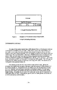
Low Temperature Growth of GaAs on Si Substrates for Ultra-fast Photoconductive Switches Kai Ma, Ryohei Urata, David A. B. Miller and James S. Harris, Jr., Solid State and Photonics Laboratory, Stanford University, Stanford, CA 94305, U.S.A. ABSTRACT We have grown GaAs directly on silicon substrates by molecular beam epitaxy (MBE) at low substrate temperatures (~250 °C). The silicon wafer surface cleaning and GaAs film growth processes were done at temperatures lower than the Si-Al eutectic temperature, in order to enable monolithic integration of low-temperature-grown-GaAs (LT-GaAs) photoconductive switches with Si-CMOS circuits. In situ reflection high-energy electron diffraction (RHEED), ex situ xray diffraction (XRD) and atomic force microscopy (AFM) studies were performed to characterize the LT-GaAs film quality. The film surfaces show less than 1 nm root-mean-square (rms) roughness and the anti-phase domain (APD) density is below the XRD detection limit. Metal-semiconductor-metal (MSM) photoconductive switches were made using this material. A time-resolved electro-optic sampling technique was used to determine the responsivity and speed of the switches. A full-width at half-maximum (FWHM) switching time of ~2 picoseconds was achieved and the responsivity of switches made from LT-GaAs on Si material was comparable to that of switches made from LT-GaAs on GaAs material. INTRODUCTION The growing need for bandwidth in optical communications and high-speed instrumentation calls for analog-to-digital (A/D) converters with bandwidths up to several tens of GHz. Previously, we proposed a photonic A/D conversion system utilizing a sample-and-hold scheme with LT-GaAs MSM switches [1]. In our system, the switches would be triggered by a fs order optical pulse in order to achieve ultra-high input bandwidth. The details of our A/D conversion system can be found elsewhere [1, 2]. LT-GaAs material is usually grown by MBE at temperatures as low as 200 °C to 350 °C, compared to conventional GaAs which is grown at 550-650 °C. LT-GaAs is highly nonstoichiometric, with 1~2 at% excess arsenic in the GaAs matrix. The high concentration of arsenic-related defects results in ultra-short carrier lifetime [3]. A high temperature post-growth anneal at above 600 °C is usually needed to increase the carrier mobility, but not substantially increase the lifetime. The LT-GaAs material was chosen to make the switches in our system because of its pico- or subpico-second carrier lifetime that allows for ultra-fast switching, reasonably high mobility to provide good switch responsivity, as well as high dark resistivity and high breakdown field [3]. Responsivity is defined here as the ratio between the amount of output charge and the number of input photons. One of the key innovations of our work is the monolithic integration of high-speed LT-GaAs photoconductive switches with low power Si CMOS integrated circuits. We have previously used a flip-chip bonding method for integration [2]. An alternative approach is to finish the final level m
Data Loading...


