Low Temperature Silicon Epitaxial Growth by Plasma Enhanced Chemical Vapor Deposition from SiH 4 /He/H 2
- PDF / 1,982,485 Bytes
- 4 Pages / 420.48 x 639 pts Page_size
- 14 Downloads / 331 Views
LOW TEMPERATURE SILICON EPITAXIAL GROWTH BY PLASMA ENHANCED CHEMICAL VAPOR DEPOSITION FROM SiH 4 /He/H 2 *
*
**
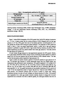
YUNG-JEN LIN, MING-DENG SHIEH, CHIAPYING LEE , AND TRI-RUNG YEW *: Materials Science Center, National Tsing-Hua University, Hsinchu, Taiwan, ROC **: Department of Chemical Engineering, National Taiwan Institute of Technology, Taipei, Taiwan, ROC ABSTRACT Silicon epitaxial growth on silicon wafers were investigated by using plasma enhanced chemical vapor deposition from SiH 4/He/H 2 . The epitaxial layers were growm at temperatures of 350'C or lower. The base pressure of the chamber was greater than 2 x 10⁻⁵ Torr. Prior to epitaxial growth, the wafer was in-situ cleaned by H2 baking for 30 min. The epi/substrate interface and epitaxial layers were observed by cross-sectional transmission electron microscopy (XTEM). Finally, the influence of the ex-situ and in-situ cleaning processes on the qualities of the interface and epitaxial layers was discussed in detail. I. INTRODUCTION During the past few years, efforts have been placed on developing low temperature epitaxial growth to minimize autodoping and solid-state diffusion effects of dopants for future bipolar and complementary metal-oxide-semiconductor techniques [1). In order to achieve low temperature epitaxy, low pressure systems were developed. Molecular beam epitaxy (MBE), one of the promising methods, has been proposed as a possible low temperature silicon epitaxial technology [21. However, the deposition temperature was still high. Chemical vapor deposition (CVD) methods are the other potential approaches for the low temperature epitaxial growth. Recently, it has been reported that the epitaxial film could be achieved from a SiH 4/SiH 2F2 /H 2 gas mixture using photo-CVD method at 250'C [3]. In addition, epitaxial film could be obtained from °C[4]_ a SiH 4 /SiF 4/H 2 gas mixture using plasma enhanced CVD (PECVD) method at 200 In this paper, silicon epitaxial growth on silicon wafers using PECVD from SiH 4/He/H 2 at 350'C or lower was investigated. The pre-epitaxial in-situ cleaning process was carried out by H2 baking prior to deposition. The influnece of the ex-situ and in-situ cleaning processes on the qualities of the interface and epitaxial layers was discussed. II. EXPERIMENTAL PROCEDURES The reactor used in this experiment is of a flat-bed, parallel planar type consisting of two electrodes, separated by 3.2 cm, to couple the RF plasma. A diffusion pump was connected to pump the chamber to a base pressure of 2 x 10 -5Torr and was shut off prior to the epitaxial growth. The reactive gas pumping system is composed of a mechanical roots pump and a rotary pump that can keep the reaction gas in the chamber in a wild pressure range. A silicon wafer, (100) oriented, p-type with a resistivity of 2-5 ohm-cm, cut to 15 mm x 30 mm, was used as a substrate for epitaxial growth. The wafer was ex-situ cleaned by spin-etch methods [5] for hydrogen passivation, which included boiling in H2 SO4/H 20 2 and spin-dry with the introduction of C2HsOH/HF/H 20. The
Data Loading...