Silicon Nanowires Obtained by Low Temperature Plasma-Based Chemical Vapor Deposition.
- PDF / 305,577 Bytes
- 6 Pages / 432 x 648 pts Page_size
- 31 Downloads / 328 Views
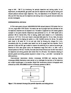
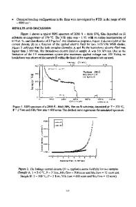
Silicon Nanowires Obtained by Low Temperature Plasma-Based Chemical Vapor Deposition. R. A. Puglisi*, G. Mannino, S. Scalese, A. La Magna Consiglio Nazionale delle Ricerche, Istituto per la Microelettronica e Microsistemi, Strada Ottava 5 Zona Industriale, 95121, Catania, Italy V. Privitera MATIS-IMM-CNR, Via Santa Sofia 64, Catania, Italy *Corresponding author: Email: [email protected], Tel.: +39 0955968237, Fax: + 39 0955968312 ABSTRACT Silicon Nanowires (Si-NWs) are obtained by vapor-liquid-solid growth using an inductively coupled chemical vapor deposition system which works at temperatures lower than 400 °C. Gold nanodots are used as metal catalyst. The selective growth of Si-NWs on the gold nanodots is obtained by controlling the contribution coming from the uncatalyzed growth on the bare Si substrate. In this way the final NW length can be controlled, and it is not influenced by the thickness of the uncatalyzed layer. The important parameter ruling the NW growth is found to be the plasma power which governs the dissociation of the Si precursor gas. Final NW lengths of 1 ȝm are obtained at temperatures of 380 °C with a thickness of uncatalyzed layer equal to zero. Also the NW density is addressed in this work and it is optimised by increasing the gold equivalent thickness. The NW density is increased from 2.9×10⁸ to 1.3×1010 cm-2, when the gold equivalent thickness passes from 1.8 nm to 2.2 nm. INTRODUCTION Standard planar junctions of Si based solar cells suffer from low efficiency/cost ratio for many reasons mainly related to the capture and conversion of the solar energy and to the high manufacturing and production costs. The intrinsic nature of the planar junction is indicated as one of the possible reasons for the low conversion efficiency because in this architecture the charge carriers are collected along the same direction as light is absorbed [1]. Radial junctions formed in quasi one-dimensional (1D) structures can overcome this limitation because thanks to their innovative architecture they orthogonalise the light absorption from the carrier collection paths, enabling at the same time to increase the first parameter and reduce the second one. In this way the requirements about the electronic quality of the material used can be lowered and the costs decreased. Si-NWs are currently considered good potential candidates for the formation of radial junctions. Besides the light/current decoupling, they offer additional advantages like reduced light reflection, improved light trapping and the possibility to tune the band-gap [2-5]. For this application however the main Si-NWs morphological characteristics such as length, diameter and density have to be controlled and optimised. One of the most popular methods to form NWs is the vapor-liquid-solid growth on metallic catalysts [6-11]. In this method the Si precursors are deposited on the substrate where they can interact with i) the catalyst, and give rise to the formation of the NW, or ii) with the bare Si substrate, where they can diffuse or form a
Data Loading...