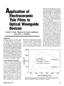
Magnetooptic Waveguide Material Structures and Devices
- PDF / 1,117,087 Bytes
- 8 Pages / 417.6 x 639 pts Page_size
- 61 Downloads / 362 Views
switching, and 4.High-speed wideband optical frequency shifting and modulation.
163
Mat. Res. Soc. Symp. Proc. Vol. 597 ©2000 Materials Research Society
In this paper, recent advances in the preparation of Ce-substituted (doped) YIG films on GGG and semiconductor substrates, hybrid material structures and the resulting microwave and MO devices, and their potential applications are presented. WAVEGUIDE MATERIALS PREPARATION Among the various insulating, ferroelectric, and semiconducting substrate materials that have been utilized for construction of guided-wave AO devices [3], LiNbO 3 and InGaAsP material system continue to be the two with the highest potential for realization of integrated AO device modules for information processing and communications. Recent progress on lasers and amplifiers in Er-doped LiNbO 3 substrate has significantly enhanced the prospects for realization of LiNbO 3-based monolithic integrated AO signal processor circuits. Similarly, continued success on construction of photonic integrated circuits (PIC) in the InGaAsP material system [4] will also expedite the same realization [3]. As to the materials for guided-wave MO devices, YIG/GGG with pure and Bi-substituted YIG [5] have been most commonly used heretofore. It is to be noted, however, that Ce-substituted YIG has recently been shown to provide significantly higher MO effects than pure and Bi-substituted YIG [6]. The prospects for incorporating lasers in the YIG/GGG substrate with doping such as Er ions have also started to be recognized. Despite the lack of alternative to the basic YIG films at present significant advances in terms of the deposition techniques, doping (or substitution) in YIG films, and the substrate materials are being made. In this section two relatively new techniques are described. Metalorganic Chemical Vapor Deposition (MOCVD) Technique YIG films have been prppared using various techniques such as sputtering, liquid phase epitaxy (LPE), vapor phase epitaxy (VPE), and pulsed laser deposition (PLD). The MOCVD technique was used for deposition of YIG films at a low deposition temperature as a function of the composition. Note that a high deposition temperature is required in the conventional LPE, which is capable of producing high quality epitaxial single crystal waveguide YIG films. The samples with high Ce concentration (for substitutions of yttrium ions Y) have been grown on lattice-matched GGG substrate at a relatively low temperature (around 600'C) and have shown excellent magnetic and optical properties as well as large MO (e.g. Faraday rotation) effects [6]. Furthermore, high quality YIG films have been grown on semiconducting substrates such as GaAs, InP and Si via MgO buffer layer at a low substrate temperature [6]. Note that the MgO buffer layer deters the decomposition and chemical reaction of the semiconducting substrates.
Pulsed Laser Deposition Technique Bismuth-substituted YIG films were previously prepared by laser ablation [7]. Cesubstituted YIG films have also been grown on (111) GGG substrates
Data Loading...