Material Removal Simulation in Sawing Processes of Photovoltaic Silicon
- PDF / 1,173,858 Bytes
- 8 Pages / 432 x 648 pts Page_size
- 93 Downloads / 342 Views
MRS Advances © 2019 Materials Research Society DOI: 10.1557/adv.2019.95
Material Removal Simulation in Sawing Processes of Photovoltaic Silicon F. Wallburg1,2,3, M. Kuna3 and S. Schoenfelder1,2 1 Leipzig University of Applied Sciences, Faculty of Mechanical and Energy Engineering, Leipzig, Germany
2
Fraunhofer Center for Silicon Photovoltaics CSP, 06120 Halle (Saale), Germany
3
TU Bergakademie Freiberg, Institute of Mechanics and Fluid Dynamics, 09599 Freiberg, Germany
ABSTRACT
The wafering of thin silicon substrates is done by wire sawing technology. In this work a numerical model for the investigation of microstructural mechanisms like cracking and damage evolution during the sawing process is presented. A three-dimensional finite element model representing the phase transformation properties of silicon is validated by loading curves from nano-indentation experiments. By using cohesive zone finite elements, the crack lengths as well as crack initiation depths can be quantified and compared with the experimental results in terms of the maximum depth of subsurface damage.
INTRODUCTION The mass production of silicon wafers, the basic substrates of solar cells, is realised with the multi-wire sawing technology in which the wafers are sawn from highpurity silicon bricks [1]. There are different wire sawing technologies available, either with fixed abrasive (diamonds on wire) or loose abrasives in a slurry. This work analyses the fixed abrasive process, i.e. diamond wire sawing. In crystalline photovoltaics, the wafering processes and the material costs represent a considerable cost share of about 40% of the complete photovoltaic module [2]. During wire sawing material removal mechanisms resulting from the interaction between hard cutting particles and the silicon surface are of great importance regarding the reliability of the processes and the quality of the products. From a manufacturing
Downloaded from https://www.cambridge.org/core. Iowa State University Library, on 06 Feb 2019 at 15:55:42, subject to the Cambridge Core terms of use, available at https://www.cambridge.org/core/terms. https://doi.org/10.1557/adv.2019.95
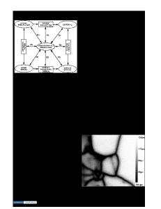
point of view, the derived goal is to achieve a high material removal rate in sawing direction while keeping the remaining damage zone in near-surface region of the wafers as small as possible. This requires a deep understanding of the development and interaction of micro cracks. During sawing of brittle silicon fracture occurs around socalled transformation zones (see Fig. 1a). Whenever abrasive particles penetrate the silicon surface, cracks are formed under the indenter edges near the surface (radial crack regime, depicted in Fig. 1b) and/or – depending on the stress scenario – below these zones (median crack regime, see Fig. 1c). The lateral crack system (illustrated in Fig. 1d), which is mainly responsible for the material removal, is formed in the unloading phase, i.e. when the pressure of the penetrating particle decreases. An excellent overview of indentation induced cracking mech
Data Loading...