Material Issues in the Commercialization of Amorphous Silicon Alloy Thin-Film Photovoltaic Technology
- PDF / 1,227,831 Bytes
- 7 Pages / 414.72 x 648 pts Page_size
- 23 Downloads / 331 Views
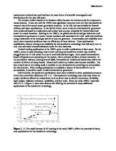
yield. The design of the cell and the method of manufacturing must be chosen keeping the above considerations in mind. CELL STRUCTURE a-Si alloy cells can be made using many different configurations (Fig. 1). A singlejunction cell is the simplest to make and consists of three layers deposited on a substrate predeposited with a back reflector. The double-junction cell may use the same material for both the component cells. Another alternative is to use a-SiGe alloy for the bottom cell to increase the long wavelength response. Similarly, for the triple-junction structure, the middle and the bottom cells use a-SiGe alloy. Ag
Ag
_ ] ITO P
F
Ag
A
Ag
Ag [TO P
P
Ag
Ag p
a-ialoy
ia-Si alloy
n Zinc Oxide Silver Stainless Steel Single - Junction
Fig. 1.
i a-Si alloy
i a-Si alloy
nP
nP
ia-SiGe n alloy
i a-Si alloy
i a-SiGe alloy
i a-SiGe alloy n Zinc Oxide Silver
-n
n Zinc Oxide Silver
Zinc Oxide
Stainless Steel Double - Junction Same Gap
n
_P _
Silver Stainless Steel
Stainless Steel
Double - Junction
Triple - Junction
Dual Gap
Multi Gap
Schematic diagram of different cell structures.
The highest stable active-area cell efficiencies for the different structures as obtained by United Solar are shown in Table I. All these values represent world record efficiencies. We see from Table I that the highest cell efficiency obtained using a single-junction structure is 9.3%. As one goes from the single-junction to the same bandgap double-junction structure, the efficiency improves to 10.1%. Incorporation of Ge in the bottom cell further improves the efficiency to 11.2%. Finally, use of a triple-junction, triple-bandgap structure results in an efficiency of 13%. In order to decide which cell structure should be chosen for manufacturing, feedback was obtained from the marketing group. From a footprint consideration, it was suggested that customers would like to see a minimum module efficiency of 8%. The cell efficiencies shown in Table I are the best results on small-area (0.25 cm 2) cells. There are many derating factors as one moves from the R&D active-area cell results to those for large-area products. Shadow and electrical losses due to the grids can amount to 7%; encapsulation losses are typically 4%. The highest quality cells are usually made at deposition rates of about 0.1 nm/sec. If a higher deposition rate is to be used for improving the throughput, an additional 10% loss in efficiency is to be expected. Moreover, translation from small-area best to largearea average can cause another 10-15% loss in efficiency. It was, therefore, felt that the triplejunction structure will offer the highest possibility of meeting the stable module efficiency goal of 8%.
100
Table I.
Highest stable cell efficiencies reported by United Solar for different cell structures.
Cell Structure
J. (mA/cm 2)
V. (V)
FF
Stable Efficiency
Single-junction
14.36
0.965
0.672
9.3%
Double-junction, same bandgap
7.9
1.83
0.70
10.1%
Double-junction, dual bandgap
10.61
1.61
0.66
11.2%
Triple-junction, mu
Data Loading...