Materials and Interface Optimization of Heterojunction Silicon (HIT) Solar Cells Using in-situ Real-Time Spectroscopic E
- PDF / 1,117,375 Bytes
- 6 Pages / 612 x 792 pts (letter) Page_size
- 54 Downloads / 262 Views
A8.3.1
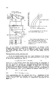
Materials and Interface Optimization of Heterojunction Silicon (HIT) Solar Cells Using insitu Real-Time Spectroscopic Ellipsometry D.H. Levi, C.W. Teplin, E. Iwaniczko, R.K. Ahrenkiel, H.M. Branz, M.R. Page, Y. Yan, Q. Wang and T.H. Wang National Renewable Energy Laboratory, 1617 Cole Blvd., Golden, CO, 80401, USA ABSTRACT We have applied real-time spectroscopic ellipsometry (RTSE) as both an in-situ diagnostic and post-growth analysis tool for hydrogenated amorphous silicon (a-Si:H)/crystalline silicon (c-Si) heterojunction with intrinsic thin-layer (HIT) solar cells grown by hot-wire chemical vapor deposition. RTSE enables precise thickness control of the 5 to 25 nm layers used in these devices, as well as monitoring crystallinity and surface roughness in real time. Utilizing RTSE feedback, but without extensive optimization, we have achieved a photovoltaic energy conversion efficiency of 14.1% on an Al-backed p-type Czochralski c-Si wafer coated with thin i and n layers on the front. Open-circuit voltages above 620 mV indicate effective passivation of the c-Si surface by the a-Si:H intrinsic layer. Lifetime measurements using resonant coupled photoconductive decay indicate that surface recombination velocities can approach 1 cm/s. RTSE and transmission electron microscopy show that the intrinsic a-Si:H i-layers grow as a mixture of amorphous and nano-crystalline silicon. INTRODUCTION Heterojunction with intrinsic thin layer (HIT) solar cells, pioneered by Sanyo Corporation, [1] show great promise for low-cost production of high efficiency solar cells. By depositing thin intrinsic and doped amorphous layers on a crystalline silicon (c-Si) substrate, it is possible to achieve very high junction quality and interface passivation using a relatively low temperature deposition process. This process makes it possible to achieve high efficiency using Czochralski (CZ) silicon by avoiding material-degrading high temperatures. The highest efficiency attained for this type of cell is 21% [2] on an n-type CZ silicon wafer with a double-sided heterojunction structure. The highest efficiency obtained on a p-type CZ wafer has been 14.2%, with an open circuit voltage (Voc) of 612 mV [3]. It is believed that the large difference in efficiencies obtained for p- vs. n-type wafers is due to the higher band offset in the minority carrier band in the case of the p-type a-Si:H/n-type c-Si heterojunction, leading to a more efficient passivation of the a-Si:H – c-Si interface [4]. Using hot-wire chemical vapor deposition (HWVCD), we have fabricated n-type hydrogenated amorphous silicon (a-Si:H) emitter on p-type c-Si wafer solar cells with efficiencies as high as 14.1% and Voc of 627 mV. We have examined a range of deposition temperatures and layer thicknesses. We have also grown a series of diagnostic structures consisting of i- and n-layers deposited on both sides of the wafer in order to accurately measure surface recombination velocities using resonant coupled photoconductive decay (RCPCD). An integral part of this research ef
Data Loading...