Materials Optimization for Silicon Heterojunction Solar Cells Using Spectroscopic Ellipsometry
- PDF / 257,408 Bytes
- 6 Pages / 612 x 792 pts (letter) Page_size
- 22 Downloads / 430 Views
0989-A24-04
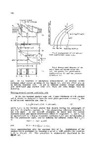
Materials Optimization for Silicon Heterojunction Solar Cells using Spectroscopic Ellipsometry Dean Levi, Eugene Iwanizcko, Steve Johnston, Qi Wang, and Howard M Branz National Renewable Energy Lab, 1617 Cole Blvd., Golden, CO, 80401 ABSTRACT We have used hot wire chemical vapor deposition (HWCVD) to fabricate silicon heterojunction (SHJ) solar cells on p-type FZ silicon substrates with efficiencies as high as 18.2%. The best cells are deposited on anisotropically-textured (100) silicon substrates where an etching process creates pyramidal facets with (111) crystal faces. Texturing increases Jsc through enhanced light trapping, yet our highest Voc devices are deposited on un-textured (100) substrates. One of the key factors in maximizing the efficiency of our SHJ devices is the process of optimization of the material properties of the 3 ñ 5 nm thick hydrogenated amorphous silicon (a-Si:H) layers used to create the junction and back contact in these cells. Such optimization is technically challenging because of the difficulty in measuring the properties of extremely thin layers. In this study, we have utilized spectroscopic ellipsometry (SE) and photoconductivity decay to conclude that a-Si:H films grown on (111) substrates are substantially similar to films grown on (100) substrates. In addition, analysis of the substrate temperature dependence of surface roughness evolution reveals a substrate-independent mechanism of surface smoothening with an activation energy of 0.28 eV. Analysis of the substrate temperature dependence of surface passivation reveals a passivation mechanism with an activation energy of 0.63 eV. INTRODUCTION Silicon heterojunction solar cells (SHJ), first called HIT (heterojunction with intrinsic thin layer) cells by Sanyo Corp., incorporate amorphous silicon contacts on crystal silicon (c-Si) to produce high efficiency c-Si cells with relatively simple, low temperature processing [1]. Extremely thin layers of intrinsic and doped amorphous hydrogenated silicon (a-Si:H) are deposited onto a c-Si wafer to passivate the wafer surfaces while also creating an electrical junction for carrier collection. These devices present unique challenges for characterization and optimization because of the extremely thin layers used in their fabrication. The SHJ devices under development at NREL use 40≈ intrinsic layers and 60≈ doped layers deposited by hot wire chemical vapor deposition (HWCVD) [2]. Our research team has demonstrated increasing Voc for SHJ solar cells as progress has been made in both materials optimization and substrate cleaning [3]. The increase in Voc has been correlated to reduced density of interface states at the a-Si:H ñ c-Si interface and reduced surface recombination (SRV) at that interface [4]. Nearly all of our materials optimization studies have focused on a-Si:H grown on (100) c-Si surfaces. Recently our team has begun to fabricate SHJ devices on textured wafers in order to increase the short circuit current (Jsc) through reduced reflection. This has produced a new recor
Data Loading...