MBE Growth of GaN on NdGaO 3 (101)
- PDF / 1,559,350 Bytes
- 6 Pages / 414.72 x 648 pts Page_size
- 81 Downloads / 289 Views
Institute of Electronic Materials Technology, ul. W61czyfiska 133, 01-919 Warsaw 118, POLAND Institute of Experimental Physics, Warsaw University, Hozia 69, 00-681 Warsaw, POLAND
3
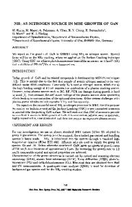
ABSTRACT We report on the growth of GaN on NdGaO3 (101) by plasma assisted molecular beam epitaxy (MBE). NdGaO3 (101) is an interesting alternative substrate compared to A120 3 due to its smaller lattice mismatch of +1.2 % to hexagonal (0001) GaN. Using photoluminescence (PL), X-ray diffraction (XRD), reflection high energy electron diffraction (RHEED) and atomic force microscopy (AFM) the optical and structural properties of the GaN thin films grown on NdGaO 3 are investigated and compared to those grown on c-plane sapphire. The intended epitaxial relationship of [0001] GaN I1[101] GaN is hard to realise as confirmed by several tilted or even polycrystalline films. However, the layer quality was found to improve considerably, when the NdGaO3 surface showed a (l x 1) instead of other reconstructions. INTRODUCTION Over the last years GaN has attracted a lot of attention as a material for optoelectronic and highpower devices. Although highly efficient blue light emitting diodes and laser diodes have been grown on (0001) oriented sapphire [1, 2], the defect density in those structures is still very high due to the lattice mismatch of 16.1 %between GaN and A12 0 3 . A reduction of defects by better lattice matched substrates is believed to improve device performance. In the past SiC [3], ZnO [4] and also MgA120 4 [5] with respective lattice mismatches of -3.01 %, +1.9 % and -9.5 % have been tried. However, results are still falling short of the ones achieved on A12 0 3 (0001). Therefore the use of new substrates with even smaller lattice mismatches like LiA1O 3 [6], LiGaO3 [7] and also NdGaO3 [8, 9] has been proposed. High quality NdGaO3 is available in 2" wafer size, as it is widely used as a substrate for the growth of high T. superconductors. First growth experiments of GaN using hydride vapour phase epitaxy [8] and metalorganic vapour phase epitaxy [9] showed promising results. NEODYMIUM GALLATE SUBSTRATE The orthorhombic crystal structure of NdGaO3 with the lattice constants and thermal expansion coefficients [10, 11] from Table I can be seen in Fig. 1. Since a is almost equivalent to b and a2 + b2 is approximately c2 this structure is sometimes called quasi-cubic. The (101) and (011) surfaces consist either of gallium or neodymium - oxygen planes, corresponding to the (111) plane of a cubic crystal structure. Therefore they should be suitable for the growth of GaN in the (0001) orientation.
295 Mat. Res. Soc. Symp. Proc. Vol. 482 ©1998Materials Research Society
Nd *Ga
* ..
9
.
S...
.
[11"OJ, GaN/[13i]
"
..........
S. .. * .
C
O
Space group Lattice constants
a [A] b [A] c [A] Lattice mismatch in %
(186) 3.189
(167) 4.758
5.189 -
12.99 +16.1
a [10-6K-1]
5.6
7.5
expansion coefficients
P [10-6K-'] q/ [10-'K-']
3.17
8.5
%
-
-25
Thermal
mismatch to GaN
Table I: Comparison of A1203
(0001)
NdGaO.
of GaN
T
Data Loading...