Measurement and Modeling of Intrinsic Stresses in CVD W Lines
- PDF / 1,525,892 Bytes
- 5 Pages / 414.72 x 648 pts Page_size
- 59 Downloads / 352 Views
been developed and successfully applied to aluminum (Al) and copper (Cu) thin films[I-6]. Although these measurements significantly contributed to the understanding of thin film stresses, the detailed stress distributions within a material could not be determined. Since it is desirable to determine the local stress distribution in complex multi-layer interconnection structures, extensive FEM modeling has been done[7-9]. Previous models were mainly limited to calculations of thermally-induced mechanical stress, since film growth stresses (intrinsic stresses) were assumed negligible in Al and Cu. This assumption is not valid for refractory metals such as W. Wafer curvature measurements have shown that thermal stress is not the major source of film stress for W, but rather, the major contribution is due to non-equilibrium film growth[10]. The W cannot rearrange itself into an equilibrium state after reaction products leave the film, so that hydrostatic growth strains result[ 11]. In this paper we present X-ray determinations of stresses in CVD W films and lines with different aspect ratios. Strains measured by X-ray were converted to stresses using Young's modulus and Poisson's ratio of 407 GPa and 0.281, respectively. We then explain how to apply FEM to the simulation of the combined effects of intrinsic and thermal stresses. Modeling results are in good agreement with measured stresses. The films are in very high tension, on the order of I GPa. About two thirds of this value is due to non-equilibrium film growth, i.e. intrinsic stress. 115
Mat. Res. Soc. Symp. Proc. Vol. 391 01995 Materials Research Society
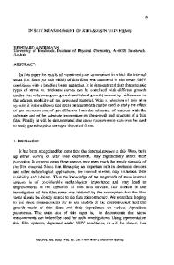
SAMPLE PREPARATION AND STRESS MEASUREMENT Blanket W films were deposited, by CVD, on multi-layered metal stacks. W line samples were generated by depositing CVD W into an array of trenches etched in Si0 2 over Al. An Al layer was deposited over the W lines. Figure 1 shows cross sections (SEM) of three samples of W lines with varying degrees of trench filling. The triangular depression at the top of each line is probably a result of slight overetching during processing. It is clear from the micrographs that there are separate regions of W growth: one region starting from the bottom of the trench and growing vertically; the others starting from the sides and growing horizontally. Since the component of stress normal to a growing surface is necessarily zero, the stress and strain tensors in the different regions must be quite different.
ISample A
Sample B
Sample C
Figure 1: Cross sections of W line arrays The average elastic strains in both the uniform films and the metal lines were measured with the Generalized Focusing Diffractometer at Stanford and the stresses calculated. The biaxial stress in the uniform films was about 1100 MPa, of which about 800 MPa is intrinsic and 300 MPa is the result of the difference in thermal contraction between the W and silicon (Si) substrate during cooling from the deposition temperature[10]. The experimental results for the metal line samples are given in Table 1. FEM MODEL
Data Loading...