Measurement of shape and deformation of MEMS at the wafer level
- PDF / 5,900,315 Bytes
- 6 Pages / 612 x 792 pts (letter) Page_size
- 14 Downloads / 320 Views
A5.72.1
Measurement of shape and deformation of MEMS at the wafer level Cosme Furlong, Curtis F. Ferguson, Michael J. Melson, and Ryszard J. Pryputniewicz NEST – NanoEngineering, Science, and Technology CHSLT – Center for Holographic Studies and Laser micro-mechaTronics Mechanical Engineering Department Worcester Polytechnic Institute Worcester, MA 01609, U.S.A.
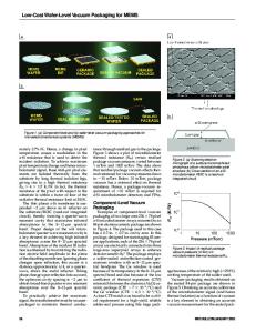
ABSTRACT One of the approaches to fabrication of MEMS involves surface micromachining to define dies on single crystal silicon wafers, dicing of the wafers to separate the dies, and electronic packaging of the individual dies. Dicing and packaging of MEMS accounts for a large fraction of the fabrication costs, therefore, nondestructive evaluation at the wafer level, before dicing, can have significant implications on improving production yield and costs. In this paper, advances in development of optoelectronic holography (OEH) techniques for nondestructive, noninvasive, full-field of view evaluation of MEMS at the wafer level are described. With OEH techniques, quantitative measurements of shape and deformation of MEMS, as related to their performance and integrity, are obtained with sub-micrometer spatial resolution and nanometer measuring accuracy. To inspect an entire wafer with OEH techniques, measurements of overlapping regions of interest (ROI) on a wafer are recorded and adjacent ROIs are stitched together through efficient 3D correlation analysis algorithms.
INTRODUCTION As the capabilities of MEMS become more widely recognized, it is also recognized that the biggest obstacle to growth of MEMS applications is the development cycle time, since it depends on tightly coordinated application of advanced design, analysis, fabrication, and testing tools [13]. Effective development of MEMS components requires synergism of advanced computeraided design (CAD), computer-aided engineering (CAE), computer-aided manufacturing (CAM) and fabrication methodologies, materials science and technology, and also of effective quantitative testing methodologies for characterizing their performance, reliability, and integrity during different phases of the electronic packaging cycle [3-6]. Testing of MEMS includes measurements of their electrical, optical, and/or mechanical responses to the driving signals and/or environmental/loading conditions. Furthermore, in order to understand mechanics of MEMS and materials used for their fabrication, advanced noninvasive testing methodologies, capable of measuring the shape and changes in states of deformation of MEMS structures and materials subjected to actual operating conditions, are required [4-7]. In this paper, we present advances in the development of optoelectronic methodologies for measuring, at the wafer level, shape and changes in states of deformation of MEMS structures with sub-micrometer resolution and nanometer measuring accuracy. To facilitate effective characterizations, the described optoelectronic methodologies incorporate [5]:
A5.72.2
(1) imaging systems based on high-spatial, high-frame rate, and high-digi
Data Loading...