Measurement of the thermal conductivity of thin layers using a scanning thermal microscope
- PDF / 1,027,287 Bytes
- 14 Pages / 612 x 792 pts (letter) Page_size
- 62 Downloads / 347 Views
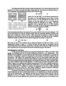
A scanning thermal microscope (SThM) was used to measure the thermal conductivity of thin sputter-deposited films in the thickness range of 10 nm–10 m. The SThM method is based on a heated tip that is scanned across the surface of a sample. The heat flowing into the sample is correlated to the local thermal conductivity of the sample. Issues like the contact force, the surface roughness of the sample, and tip degradation, which determine to a great extent the contact area between tip and surface, and thus the heat flow to the sample, are addressed in the paper. A calibration curve was measured from known reference materials to quantify the sample heat flow. This calibration was used to determine the effective thermal conductivity of samples. Further, the heat diffusion through a layered sample due to a surface heat source was analyzed with an analytical and numerical model. Measurements were performed with films of aluminum, ZnS–SiO2, and GeSbTe phase change material of variable thickness and sputter-deposited on substrates of glass, silicon, or polycarbonate. It is shown in the paper that the SThM is a suitable tool to visualize relative differences in thermal structure of nanometer resolution. Determination of the thermal conductivity of thin layers is possible for layers in the micrometer range. It is concluded that the SThM is not sensitive enough to measure accurately the thermal conductivity of thin films in the nanometer range. Suggestions for improvement of the SThM method are given.
I. INTRODUCTION
Thin layers are used in a wide range of technical applications in which their thermal properties (thermal conductivity and heat capacity) are of functional importance, for example in microelectronics, solid-state data storage, and optical disks. For example, in optical phase change disks, phase transitions, i.e., the writing and erasure of data, are thermally induced by a focused laser spot. The performance of the write and erase processes is to a great extent determined by the thermal properties of the thin films present in the recording stack. Another example is the temperature control of microelectronics. Local overheating of critical components may lead to early drop-out of devices. The usage of heat conducting interfacial layers may improve the heat removal from critical components and therefore lead to an improved lifetime cycle of the device. The thermal conductivity of thin layers may be significantly lower than that of bulk materials due to structural disorder and interfacial barriers which restrict beneficial phonon and electron transport through and across the layer. Such structure defects can for example be caused by the deposition process. The growth process 2530
http://journals.cambridge.org
J. Mater. Res., Vol. 16, No. 9, Sep 2001 Downloaded: 13 Mar 2015
may also lead to an anisotropic thermal conductivity. It is for example well known that sputtered metal films have typically columnar structures.1,2 The gaps between the columns prevent a favorable heat diffusion in the inplane direction whi
Data Loading...


