Resistometric Mapping using a Scanning Tunneling Microscope
- PDF / 2,060,203 Bytes
- 6 Pages / 414.72 x 648 pts Page_size
- 83 Downloads / 387 Views
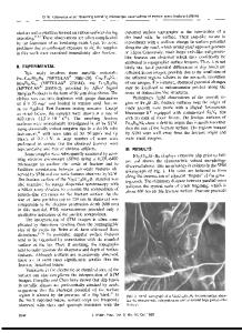
with the use of STM to measure electrochemical potentials [6], or Kelvin probe mapping, in which the surface potential variations resulting from changes in work function are mapped [7].) In this paper we present a development of the STP technique which expands the scope of application to include bulk conductive specimens and also materials exhibiting resistive anisotropy. Our method of resistometric mapping (so called to emphasis our interest in resistivity and to distinguish it from other potentiostatic techniques, mentioned above, which are becoming common in probe microscopy) has been successfully applied to a range of materials. Results are presented from representative specimens. The technique lends itself not only to investigations of microstructural influences on resistivity, but also to non-destructive detection of subsurface features. In addition, resistometric scanning offers promise as a technique for identifying lowresistivity paths in a material, for characterization or optimization purposes. EXPERIMENT The technique The technique uses a standard STM with the addition of AC bias and demodulation circuitry, as shown in figure 1. A conventional DC bias voltage is applied between the specimen surface and the STM tip. An AC voltage is imposed in the plane of the specimen; a second in-plane AC voltage, geometrically orthogonal to the first and offset in frequency, may be simultaneously imposed. The tip is scanned across the specimen surface in the normal manner. Topographic information (the conventional STM scanned image) is extracted from the DC current which flows across the tunneling junction. Potentiometric information is extracted simultaneously from the inplane current (or simultaneously from two orthogonal in-plane currents) by synchronous demodulation of the tunneling current with the AC voltages. This is similar in principle to the methods used previously, but the novel use of AC potentiometric voltages significantly improves the versatility of the technique. It is possible to perform resistometry in two in-plane dimensions; and the potential and topographic information is acquired simultaneously rather than sequentially, leading to lower noise levels [5]. The system was designed to drive large, high-frequency currents through the specimen, so that detectable potential variations would be created despite the low resistance of bulk metallic specimens. It is important that the tunneling tip be positioned with exactly the same tip-to-sample separation at each point on the surface, in order to avoid artifacts arising from changes in the tunneling junction resistance. This is achieved by continuous use of conventional STM-type feedback, using a tunneling signal mutually orthogonal to the two STP signals. current amplifier
bias
bf E55 kHz1
l• "•
1:
Y surface
out
Jpotential
Figure 1: This diagram shows the resistometric scanning system. The tunneling current has three components, derived from the conventional DC bias voltage and the two in-plane AC voltages. The AC voltage at the tip is a sensitiv
Data Loading...