Measurement Technique, Oxide Thickness and Area Dependence of Soft-Breakdown
- PDF / 399,850 Bytes
- 7 Pages / 416.88 x 635.4 pts Page_size
- 72 Downloads / 300 Views
ABSTRACT For sub-5 nm oxides there are two different stages for breakdown; soft breakdown (SBD) and hard breakdown (HBD). It has been shown that both SBD and HBD exhibit the same statistics. Therefore, the physical mechanism governing them is the same. The major difference between them is the energy transferred from the capacitor to the localized conducting path. In this paper, a simple equivalent circuit is proposed to explain the effect of the measurement technique, oxide thickness, and test structure area on the detection of soft breakdown. Also an inelastic quantum tunneling model is proposed to discuss the current-voltage characteristics after SBD. The model is also successful in explaining the temperature dependence of SBD IV characteristics.
INTRODUCTION Gate oxide reliability is one of the limiting factors in the further scaling of Si technology. It is typically studied by applying a high field stress, which can be either a constant voltage stress (CVS) or a constant current stress (CCS), and observing the time-to-oxide-breakdown. During stress, microscopic defects such as interface-traps (1], neutral electron traps [2] and positive and negative charges are generated in the silicon dioxide. The generation of these defects continues until a critical density of defects is reached. At that time, a conductive path is formed in the oxide layer connecting the anode to the cathode. For sub-5 nm oxides, the formation of conducting path leads to two different modes for oxide breakdown, namely soft breakdown [3, 4, 5] and hard breakdown. In the first section of the paper it is argued that the major difference between soft breakdown and hard breakdown is the energy transferred from the capacitor to the localized conducting path. For this purpose a simple equivalent circuit is proposed to explain the effect of the measurement technique (CCS and CVS), oxide thickness, and test structure area on the detection of soft breakdown. Using this simple circuit, one can determine the area and the oxide thickness for which soft breakdown will be observed. The second section describes a new model to explain current conduction after SBD. The model is based on inelastic quantum tunneling of electrons through the traps.
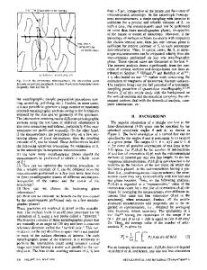
EQUIVALENT CIRCUIT FOR CCS AND CVS In Fig. 1 a simple equivalent circuit is proposed to explain the drop in voltage during CCS. In this approach the oxide resistance is considered as a very large linear resistor. The use of a nonlinear resistor has no significant influence on the general conclusions. Cox is the oxide capacitance, R, (few ohms) is the series resistance in the circuit (due to substrate and gate electrode resistance), Rtun is the tunnel resistance of the oxide and RSBD is the resistance of the localized path after SBD. 337 Mat. Res. Soc. Symp. Proc. Vol. 592 © 2000 Materials Research Society
RSBD I
Figure 1: Equivalent circuit for oxide after SBD for CCS. For the CCS an ideal current source is assumed while for CVS an ideal voltage source is used. For a fixed current density J (or current It,,,) the
Data Loading...