Mechanical response of a single and released InP membrane
- PDF / 179,472 Bytes
- 6 Pages / 612 x 792 pts (letter) Page_size
- 111 Downloads / 292 Views
1049-AA02-07
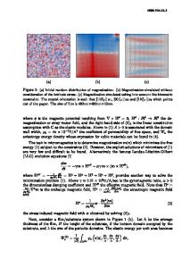
Mechanical response of a single and released InP membrane Eric Le Bourhis1, and Gilles Patriarche2 1 Laboratoire de Métallurgie Physique, Université de Poitiers, UMR 6630 CNRS, SP2MITéléport 2-Bd Marie et Pierre Curie, BP 30179, Futuroscope-chasseneuil Cedex, F-86962, France 2 Laboratoire de Photonique et de Nanostructures, CNRS UPR 20, Marcoussis, 91460, France ABSTRACT InP membranes have been microfabricated and released on top of an InP substrate. The release process comprises membrane photolithography, interlayer sacrificial etching of a InP/InGaAs/InP substructure and drying with CO2 at critical point. The mechanical response of the obtained small (40 µm) and thin (0.4 µm) membranes could be tested by nanoindentation. While keeping their epitaxial orientation through the fabrication process, delamination of the membrane was observed to occur before the indenting load reached 10 mN. Then cracking of the membrane was detected as a pop-in on the loading curves for loads larger than 10 mN. INTRODUCTION Mechanical behavior of single objects has attracted much interest in the past few years [1]. In this field, semiconductor defect and size engineering allows fabricating model structures. Moreover, indentation technique has proved to be powerful to test small volumes [2]. Originally, contact mechanics was developed for semi-infinite half space [3], this assumption being not fulfilled when the size of the plastic zone becomes of the order of one of the dimensions of the object [4-9]. ‘Small’ structures are expected to show a mechanical behavior deviating from that of a bulk. So far, length scale induced changes in the response of single semiconductor objects has been poorly addressed. Only recently were reported nanoindentation studies of GaAs single lines and of focused-ion beam (FIB) milled GaAs pillars in the µm-length scale [7-9]. Therefore, we decided to investigate the mechanical response of individual, small (40 µm in diameter) and thin (~ 0.4 µm) InP membranes. These were fabricated from InP/InGaAs/InP substructures and released on top of the InP substrate. Nanoindentation could be performed on these single membranes under increasing loads while interferential and transmission electron microscopies allowed getting deeper insight into the deformation of such small objects. EXPERIMENT Undoped (001) InP substrates were used for the study. InP membranes were micro fabricated and released on top of the InP substrate in a four step process. The first step was to grow an InP/InGaAs heterostructure on an InP substrate by low-pressure metal organic vapor phase epitaxy (MOVPE). The InGaAs layer was meant to be sacrificial and etched subsequently in order to release the membrane. Before this third step, the membranes were fabricated by photolithography of a poly-methyl methacrylate (PMMA)-based resin film previously deposited on top of the InP/InGaAs coated InP substrates. After the revealing step, a-SiN was deposited by plasma-enhanced chemical vapor deposition (PECVD). A lift-off process allowed producing
Data Loading...