Microstructural Evolution of Ion Bombarded Copper Thin Films
- PDF / 1,734,057 Bytes
- 6 Pages / 417.6 x 639 pts Page_size
- 87 Downloads / 368 Views
Max-Planck-Institut fuir Metallforschung, Seestrasse 92, D-70174 Stuttgart, Germany ABSTRACT The effect of low-energy ion bombardment on the microstructure of copper films will be described. The copper films have been deposited on SiNx-coated, oxidized Si wafers by magnetron sputtering with a simultaneous bombardment of low-energy argon ions (60 eV). The films were annealed at 450'C in HV. The ion bombardment leads to a stronger and sharper {111 } texture of the as-deposited films. After annealing, the ion-bombarded films had a significantly smaller grain size than films produced without ion bombardment. The experimental results will be discussed relating the textures of the as-deposited films with the grain sizes obtained after annealing. Details will be given describing how the microstructure of Cu films can be tailored using low-energy argon ion bombardment. INTRODUCTION Polycrystalline metal films are of great importance for a variety of industrial applications, i.e. semiconductor, photovoltaic, data storage and automotive industries. In particular, magnetron sputtering is one of the most commonly used methods for thin film deposition due to the simplicity of the physical processes involved [1]. The microstructure of polycrystalline thin films is frequently modified by a combination of various heat treatment procedures which follow the deposition process. Typical variable deposition parameters are gas pressure, target purity, deposition rate, and substrate temperature [1]. An additional important parameter is the sputter geometry, which may support growth anisotropies and
,elf-
shadowing effects [2-6]. Recently, new methods involving ion beam assisted deposition (IBAD) were used to modify thin film microstructures [1, 7-8]. A promising approach to control the texture, and in particular grain size distributions, is to heat treat the films following sputtering under different ion bombardment conditions. EXPERIMENTAL Sputter Deposition Commercially prepared SiNx/SiO 2-coated single crystal (100)-oriented Si wafers were used as substrates. The thickness of the SiN, and SiO 2 was 50 nm for each film. Prior to film growth the wafers were cleaned with CO 2 gas and mounted on a Ta sample holder plate. DC magnetron sputter deposition of Cu films was performed in an UHV system with a base pressure of 107 Pa. For deposition of Cu (99.999 at %), a magnetron source was used. The magnetron and ion-gun beam axis were aligned 230 to the substrate normal. Deposition was carried out at ambient temperature at a rate of lIam/h. Deposition was stopped at a final film
85 Mat. Res. Soc. Symp. Proc. Vol. 585 ©2000 Materials Research Society
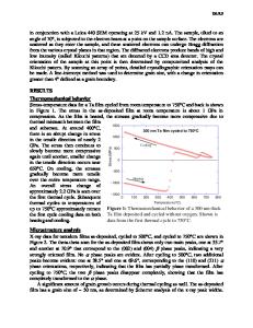
2 thickness of 1.3 pm. During deposition the ion-beam current was varied between 0 mA/cm and 2.69 x 10⁻⁵ mA/cm2 . The Ar ion energy was fixed at 60 eV. During sputtering, the substrate temperature increased from 50'C to 70'C. In the case of ion-beam bombarded films, the substrate temperature reached 100'C. After sputtering, the Cu films were annealed in a quartz tube vacuum furnace (105 mbar)
Data Loading...