Mesoscopic characterization of the optical property of antiphase boundaries in CuPt-ordered GaInP 2
- PDF / 1,834,298 Bytes
- 6 Pages / 417.6 x 639 pts Page_size
- 57 Downloads / 286 Views
ABSTRACT We have developed an apparatus for polarized cathodoluminescence (CL) spectroscopy combined with transmission electron microscopy (TEM), that enables us to obtain simultaneously structural data in higher spatial resolution by TEM and polarized luminescence spectra by CL of the same microscopic area. The polarized-CL/TEM method is very useful to study the optical properties of low-dimensional microstructures in semiconducting materials. We have applied the method to examine the optical property of antiphase boundaries in CuPt-ordered GalnP 2 and found, for the first time, the polarized light emission from the APBs whose habit planes are parallel to the (Tl 1) and (ITO) atomic planes.
1. INTRODUCTION Planar defects in semiconducting materials, such as dislocation loops and grain boundaries, are of interest because they may exhibit novel optical properties. The optical properties of these microdefects in a mesoscopic scale have been extensively studied by cathodoluminescence (CL) spectroscopy combined with transmission electron microscopy (TEM) and scanning TEM [e. g. 1-4], which enables us to obtain simultaneously structural data in higher spatial resolution by TEM and polarized luminescence spectra by CL of the same mesoscopic area. We have applied the method to examine the optical property of grain boundaries in CuPt-ordered GaInP, alloys
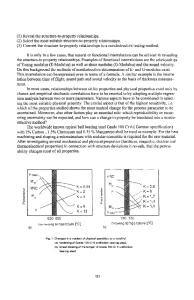
[5]. The alloys, consisting of the domains of the equivalent but mutually displaced ordered lattices bounded by antiphase boundaries (APBs) [6], usually emit the CL and PL light below the band gap energy Eg. A correlation between the light emission and the microstructures of the domains and boundaries has been studied experimentally [7-1 1] and theoretically [12]. Nevertheless, the origin of the emission lines is still unclear. We have shown that the emission arises from the specific parts of APBs. 3. EXPERIMENTS Samples were undoped GaInP 2(1 gtm thick) grown on a GaAs substrate by MOCVD; the growth temperature was 650 °C, the growth rate was 0.4 nm/s, the 111/V ratio was 370, and the substrate was 20 off from (001) towards [T"1]. Cross sections of the sample for polarized CL spectroscopy (about 300 nm in thickness) were prepared with a conventional etching method with 2-keV Ar0 ions. CL spectra at the temperature of 20 K was obtained from a sample located in an electron microscope (Fig. 1): the CL light is collected on the end of an optical fiber with an ellipsoidal mirror and the corrected light is introduced in a monochromator through the optical fiber [13].
105 Mat. Res. Soc. Symp. Proc. Vol. 588 ©2000 Materials Research Society
Optical-fiber (depolarizer)
I I Ellipsoidal-mirror
4S
polarized-CL
spectra
ple
Optical window ITEM images [TED patterns Fig. I A schematic view of an apparatus for in-situ polarized-CL spectroscopy in an transmission electron microscope. We attached a linear polarizer on the end of the optical fiber to analyze the polarization of CL. Figure 2 shows the polarized CL spectra of GaAs and GaInP 2 for four polarization directions. The e
Data Loading...