Mev Ion Induced Damages and their Annealing Behavior in Silicon
- PDF / 2,200,384 Bytes
- 6 Pages / 414.72 x 648 pts Page_size
- 53 Downloads / 292 Views
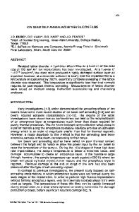
transmission electron microscopy was conducted for defect observations using a JEOL-JEM 2000 EX. The annealing behavior of ion induced defects was examined using an X-ray double crystal method. The X-ray rocking curves were recorded by rotating the sample by 1 arcsec per second. The strain depth profile was analyzed using RADS (rocking curve analysis by dynamical simulation), from the rocking curves[ 1I]. RESULTS AND DISCUSSIONS Fig. 1 shows RBS channeled spectra for the samples implanted with 2 MeV Si+ at doses of 5xl014/cm 2 and lxlO16 /cm 2 respectively. Differences in channeling yield between a virgin sample and the implanted ones are due to the existence of lattice damage induced by ion implantation. As shown in these spectra the
damaged regions are isolated from the surface
35oo
...-.....
3000 2500
2000,n random
1
2
11010(CM
and the amount of damage increases as the ion 10005 x jm/ 0 °irgi dose increases. However, near the surface viI n _g 500 already concentration damage the region, 100 1.0 200 250 300 350 50 °o saturates at a dose of 5x10¹⁴/cm 2. Fig. 2 shows a series of XTEM micrographs for the samples Channels according to ion dose variations from Fig. 1 RBS channeled spectra for the as3x1014/cm 2 to lxl016 /cm 2 implanted with 2 implanted samples according to ion dose MeV Si'. As shown in Fig. 2 (a), any variations from 5x10¹⁴/cm 2 to lx10 16/cm 2 distinctive defect region was hard to resolve using 2 MeV Six. under TEM when the ion dose reaches 3x10¹⁴/cm 2 . For the as-implanted samples beyond the dose of 5x10' 4 /cm 2, the isolated defect region begins to appear as a dark band. Results of channeled RBS indicate that a continuous amorphous layer does not yet form at a dose of lxl01'5 /cm 2 . HRTEM observations confirmed that amorphous phases in the shapes of islands are embedded in the matrix of the silicon crystal. As shown in Fig. 2 (d), as the ion dose reaches Ixl016/cm 2, a buried continuous amorphous layer is finally formed in good agreement with RBS results. The damaged region, visible as a dark band under TEM, induced by MeV implantation is isolated from the surface and concentrated around Rp as can be seen in Fig. 2 (b), (c) and (d). In the case of MeV ion implantation, electronic energy loss is prevalent near the surface region and when the ion loses its energy significantly nuclear energy loss becomes the dominant energy loss mechanism. Therefore, point defects such as Frenkel pairs are generated near the end of range much more than near the surface. Ion induced Frenkel pairs constitute a Si self interstitial and a vacancy. The spatial distribution of such an interstitial and a vacancy, however, varies along the depth of the incident ion. According to TRIM-code simulations, a vacancy rich zone is formed near the surface region while around the EOR an excess interstitial zone is located. Moreover, implanted atoms themselves, preferentially located at around Rp, contribute to additional interstitial concentration equivalent to the ion dose unless they make new lattice planes. The dark ba
Data Loading...