Defect annealing in ion implanted silicon carbide
- PDF / 205,449 Bytes
- 7 Pages / 612 x 792 pts (letter) Page_size
- 1 Downloads / 438 Views
MATERIALS RESEARCH
Welcome
Comments
Help
Defect annealing in ion implanted silicon carbide L. Calcagno, M. G. Grimaldi, and P. Musumeci Dipartimento di Fisica, Universit´a di Catania and Istituto Nazionale Fisica della Materia, C.so Italia 57, Catania, Italy (Received 29 July 1996; accepted 21 March 1997)
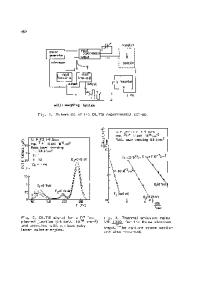
The recovery of lattice damage in ion implanted 6H-SiC single crystals by thermal annealing has been investigated in the temperature range 200–1000 ±C by Rutherford backscattering spectrometry-channeling and by optical measurements in the UV-visible wavelength. The damage was produced by implantation at room temperature of 60 keV N+ at fluences between 1014 and 5 3 1015 ionsycm2 . At low fluences a partially damaged layer with defects distributed over a depth comparable to the projected ion range was obtained. At higher fluences a continuous amorphous layer was formed. The defect annealing behavior depended on the initial damage morphology: an almost total defect recovery occurred in partially damaged layers with kinetics depending on the initial damage degree. If the defect concentration is smaller than 20 at. % the annealing rate is independent of temperature. Amorphous layers were stable in the investigated temperature range and no epitaxial regrowth occurred. After annealing, a strong change in the optical properties of the amorphous phase was observed indicating a recovery of the electronic properties of the material, suggesting the existence of several amorphous states and the relaxation of the amorphous that evolves toward thermodynamic states characterized by lower free energy values.
I. INTRODUCTION
Silicon carbide (SiC) has been intensively investigated in the last decade because of its attractive properties for electronic applications.1,2 It has been shown that some of the basic parameters of SiC devices, like the breakdown voltage and the cut-off frequency, are one order of magnitude higher than those of analogous silicon based devices. The conventional diffusion techniques are unavailable to produce SiC based devices because of the extremely high temperatures (ø2000 ±C) required for dopant diffusion.3 Ion implantation remains as an alternative doping technique. This method has been successfully utilized in the production of p-n junction diodes and field effect transistors. However, ion implantation results in a severe damage of the crystalline structure, and post-implantation annealings, at temperatures higher than 1500 ±C, are necessary in order to restore the crystallinity and to electrically activate the implanted ions.4,5 Several papers about the annealing of damage introduced by ion implantation in silicon carbide have been published.6-13 It has been shown that defect annealing is not a simple process, but it depends on the implantation details like the ion species, fluences, and substrate temperature. Bohn et al.6 observed by RBSchanneling a distinct annealing behavior of the defects in samples with different degrees of damage: the defect recovery is almost complete already at 900 ±C J. M
Data Loading...