Microcrystalline Germanium Carbide: A New, Almost Direct Gap, Thin Film Material for Photovoltaic Energy Conversion
- PDF / 113,753 Bytes
- 5 Pages / 612 x 792 pts (letter) Page_size
- 16 Downloads / 325 Views
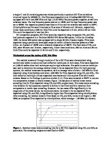
MICROCRYSTALLINE GERMANIUM CARBIDE : A NEW , ALMOST DIRECT GAP, THIN FILM MATERIAL FOR PHOTOVOLTAIC ENERGY CONVERSION Vikram L. Dalal and Jason T. Herrold Iowa State University, Dept. of Electrical and Computer Engr., Ames, Iowa 50011, USA ABSTRACT We report on the growth and electrical and optical properties of micro- and polycrystalline Ge1-x Cx films. This is a new material which does not exist in nature. The films were grown using ECR plasma techniques under conditions of low pressure and high power from a mixture of germane, methane and hydrogen. The bandgap of the material could be varied from that of c-Ge (~0.7 eV) to almost 1.15 eV by changing the methane/germane ratio. X ray diffraction and Raman measurements indicated good crystallinity in the film. The optical absorption spectrum of the film resembles that of c-Ge, with a near direct bandgap, implying that as C is added, both the central and the L valley in the conduction band move up simultaneously, while maintaining a small (~0.15 eV) separation between the two. The Hall mobility was measured to be 70 cm2/V-sec. The films were doped n- type using phosphine, and p- type using diborane. P-n junctions with good rectification characteristics were fabricated. Because of its excellent optical absorption, this material may be suitable for photovoltaic applications, particularly for tandem junction cells. We have also observed that grain size can be controlled using H etching, and have observed distinct changes in optical properties related to quantum size effects in c-Ge films. INTRODUCTION It has been known for some time that c-Ge is a reasonably good absorber of light because of a very small separation (~0.15 eV) between the lowest L valley and the central Γ valley in the conduction band[1]. As a result, it behaves almost like a direct gap semiconductor. Unfortunately, its bandgap (~0.66 eV) is too low for efficient photovoltaic energy conversion[2]. In contrast, c-Si, which has a bandgap (1.12 eV) closer to the optimum gap for PV conversion (~1.5 eV), is a very poor absorber of light because of a large ( many eV) separation between the lowest X valleys and the central Γ valley. Therefore, neither Si nor Ge can be used for efficient PV conversion in a thin film form. However, when one examines the band structures of Ge and of diamond , with a bandgap of ~5.4 eV, it becomes apparent that a small addition of C to Ge would result in a material with a bandgap in the optimum solar range, and one would only need to add a few % C to Ge to achieve such a bandgap. Upon examining the lattice constants of Ge and diamond, it also becomes apparent that the addition of a few % C to Ge would reduce the lattice constant of the material to a value close to that of c-Si, thereby making Ge1-xCx compatible with deposition on crystalline Si. Several questions remain before such a material becomes useful for PV conversion. 1. Does the band structure remain essentially that of Ge, i.e. would such a material have a high absorption characteristic of a small separation between L and
Data Loading...