Microscopic and Theoretical Investigations of the Si-SiO 2 Interface
- PDF / 1,314,076 Bytes
- 6 Pages / 412.2 x 633.6 pts Page_size
- 70 Downloads / 328 Views
"nowat: European Commission. Joint Research Centre. Institute for Advanced Materials, PO Box 2. 1755 ZG Petten. The Netherlands
15 Mat. Res. Soc. Symp. Proc. Vol. 592 ©2000 Materials Research Society
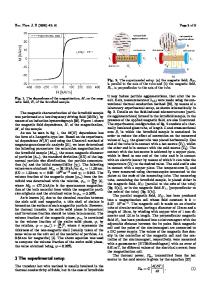
EXPERIMENT AND THEORY Two dedicated scanning transmission electron microscopes (STEM) were used to obtain atomic-resolution Z-contrast images and highly spatially resolved EELS data. Figure 1 shows the schematic of a STEM. The electron beam in a VG HB603 U (HB501 UX) with 300kV (100kV) acceleration voltage can be focused to a probe of diameter of 0.13 nm (0.22 nm). The signal of the annular detector with high inner angle (>20 mrad) is collected synchronously to the scanned beam. The image formed that way is called a Z-contrast image because the contrast is roughly proportional to the square of the mean atomic number Z in the probed volum 6. The resolution in a Z-contrast image is better than the diameter of the electron beam7 . The HB603 U is therefore sufficient to resolve the so-called dumbbell structure in silicon (0.13 nm distance between the atom columns) viewed in the (110) direction'. The images are easy to interpret as every bright spot corresponds to an atomic column Simultaneously with Z-contrast imaging, we can utilize EELS, because only electrons scattered to low angles are used for this analytical technique.
IFiAgschematic w-el: reptesenttaon of Z-con•r•t imaging and electron energy-loss
spectroscopy in a STEM
In this paper we consider the O-K ionization edge in an EELS spectrum originating from excitations from the 0 - ls state into final states with p-symmetry (because of the dipole selection rule). This technique enables investigations of the electronic structure with high spatial resolution". The photodiode used as a detector in the parallel EELS spectrometer did not allow the acquisition of spectra while the probe was held stationary because of excessive elctron beam damage. It was, therefore, necessary to use the spatial difference technique to obtain a lower dose"1 . In this technique a spectrum is taken while the beam is scanned in an area containing the interface. A reference spectrum is acquired under the same conditions in the bulk for a weighted subtraction. The result of this technique is a linear combination of the local DOS of all the atoms which differ from bulk. In order to increase sensitivity to the interfac 12we used a rectangular area with a length (parallel to the interface) of 50 nm and a width (perpendicular to the interface) of 2 nm. No electron beam damage was observed in the Z-contrast images during and after the spectrum acquisition. Ten spectra were summed up to improve the signal to noise statistics. All the spectra were inspected individually for signs of electron beam damage prior to
16
the summation. A series of interface and reference spectra (in the oxide) was obtained in random order to insure the stability of the energy scale. The C-K edge originating from a slight contamination was used to check the energy calibration. In addition to the microscopy studies, we
Data Loading...