Microstructural Characterization of Antimonide Based III-V Compounds and their Effect on Electro-Optical Properties of S
- PDF / 4,327,789 Bytes
- 12 Pages / 417.6 x 639 pts Page_size
- 85 Downloads / 240 Views
Mat. Res. Soc. Symp. Proc. Vol. 588 ©2000 Materials Research Society
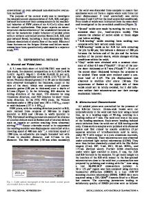
which is a common n-type dopant in antimonides. The 777 and 710 meV peaks are related to a doubly ionized native acceptor center [3]. of low combination A temperature PL and spatially resolved CL techniques is invaluable in studying the distribution of point defects in the material after any processing step. Figure 2 shows CL images and the respective spectra of GaSb annealed in Ga- and Sb- rich environment and under vacuum; such annealing is done to
C)
-C _j
a-
750
800
850
900
Photon energy (meV)
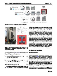
FIG. 1. PL spectra of (i) undoped p-GaSb (NA-ND = 1.2 x 1017 cm3), (ii) Te- compensated p-GaSb (NA-ND = 3.4 x 1 0 16 cm 3), (iii) Tecompensated p-GaSb (NA-ND = 1.5 x 1016 cm 3),
and (iv) Te- doped n-GaSb
(ND-NA =
2 x 10
cm 3). The carrier concentrations mentioned here are at room temperature.
188
reduce
the
number
of
native
acceptors in as-grown undoped GaSb [4]. While the defects are nonuniformly distributed in as-grown GaSb (Fig 2a), annealing treatments improve the overall uniformity of the defect complexes (Figs. 2b, 2c). The relative efficiency in point defect reduction through each annealing treatment can be evaluated from the CL spectra (Figs. 2a-2c), wherein a decrease in the relative peak intensity of the 777 meV transition is observed. Based on temperature dependent PL and CL measurements, energy level models for undoped and doped GaSb have been developed as shown in Fig. 3 (a) and (b) respectively [3-8]. The native acceptor centers associated with each of the PL transitions are indicated in the figure. The mechanisms for acceptor complex formation in GaSb as a result of impurity doping are also listed. growth from post Apart annealing treatments, efforts to reduce native defects by iso-electronic and transition metal impurity doping have been evaluated using CL measurements [5-7]. The PL and CL techniques have also been found to be extremely useful for studying passivation of antimonide surfaces and extended defects in the crystals [8-11].
d V2
(a)
1!
C. Ga annealed
.
,
. ..... ..
U
1500
1700
1600
1800
wavelength (nm)
"
--
..
i
0m
Sb annealed Ga annealed
vacuum sanealed
(c)
C-2
1500
1600
1700
wavelength (nm)
1800
FIG. 2. CL images and spectra of (a) as-grown undoped GaSb, (b) Ga- annealed and (c) Sbannealed undoped GaSb. The CL spectra were recorded at 77 K. The annealing treatments were performed at 500 'C for 12 hrs. The two CL spectra in (b) are taken from two different positions of the Ga-annealed sample. Fig. (c) also contains spectra obtained from Ga- and vacuum annealed samples for the sake of comparison.
189
3.8 meV
........................... t ............................. .......................... D+
812 meV
Te+
.............................. l ........ ..................................................... A - - (V oa-&s................................................................ 72.•..meV ....,....v ......... G.Ga~b)-72 102 meV
(V GaG aSb Tesb)" --N....................
Data Loading...