Microstructural Correlation with Electrical Properties for Y 2 O 3 Doped CeO 2 Thin Films
- PDF / 1,085,501 Bytes
- 6 Pages / 414.72 x 648 pts Page_size
- 95 Downloads / 383 Views
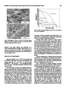
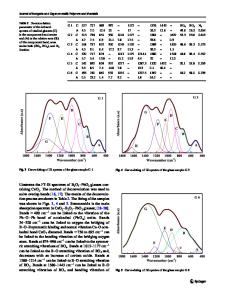
Abstract High quality textured 0.58% Y20 3 doped CeO 2 films with (001), (111)/(001) and (110) were prepared using an e-beam deposition technique on substrates of (001) LaA10 3, r-cut sapphire, and fused silica, respectively. The composition and stoichiometry of the films were verified by Rutherford backscattering spectroscopy analysis. Both x-ray diffraction and transmission electron microscopy analyses gave consistent microstructural information. Complex impedance measurements have been performed to study the electrical properties of these films as a function of temperature. The conductivities of the films were dominated by grain boundaries of high conductivities as compared to that of the bulk ceramic of the same dopant concentration. The activation energies for the film conductivities were only slightly higher than that for the bulk lattice conductivities, but much lower than that for the bulk grain boundary conductivity. These results have been discussed in terms of the differences of the grain size and grain boundary microstructures between the films and the bulk ceramics.
Introduction CeO 2 based electrolytes have been shown to have an exciting prospect when used in oxygen sensors and intermediate temperature (500-700'C) solid oxide fuel cells (SOFC) as compared to the YSZ based devices which operate at 1000°C or higher.' Furthermore, thin layers of solid electrolytes can minimize the ohmic loss in the electrolytes so as to lower the operating temperature and maintain the required power output. 2' 3' 4 Therefore, it is highly desirable to produce thin layers of these materials for solid oxide device applications. There is a well known, so-called "grain boundary effect"5 , which can lower the effective DC conductivity by 2-3 orders of magnitude6 . Several studies of this phenomenon have been done for bulk materials, but few deals with thin films. Since the ratio of grain boundary area to lattice volume in thin films is larger than that of bulk ceramics, grain boundaries will have a larger impact on film properties. Thus, it is important to understand the "grain boundary effect" in thin film electrolytes. In addition, the advantage of the microstructural engineering of thin films make it possible to correlate the microstructure with their electrical properties to optimize the film properties for device applications. Here, we prepared yttria doped ceria thin films using an electron-beam deposition technique and investigated the relation between the microstructure and the electrical properties of CeO 2 thin films.
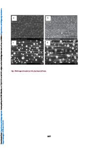
Experimental Films were grown using the electron-beam deposition technique. The film deposition parameters were described previously. 7 During deposition, oxygen was introduced to fully oxidize the films. After deposition, films were annealed and cooled to room temperature under an oxygen partial pressure (P0 2) of 10-3 Torr. The Ce, Y, and oxygen contents of the films were determined by Rutherford Backscattering Spectroscopy (RBS) with 2.275 MeV He 2÷. The microstructures of the as-deposited films w
Data Loading...